
550/100kHz Noise Measurement System
Oct 27, 2015
This article describes a noise-measurement system with an effective bandwidth of 550kHz or 100kHz.
The system can be used to measure total output noise of circuits with output impedances below about 100ohm.
A Midiman DMP3 high-gain very low noise preamplifier is used to amplify the broadband noise signal (from 3Hz to about 550kHz or 100kHz)
from the circuit to be tested. The noise output of the preamplifier is measured using a
Digilent Analog Discovery 10MHz scope
and measuring AC rms volts. The configuration is shown below:
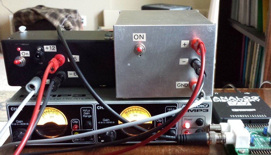
DMP3 Preamplifier
The DMP3 preamplifier, a dual-channel very low noise microphone preamplifier, uses a INA163 low-noise instrumentation amplifier (with ~ 1.0nV/√Hz noise voltage). One channel of the DMP3 is
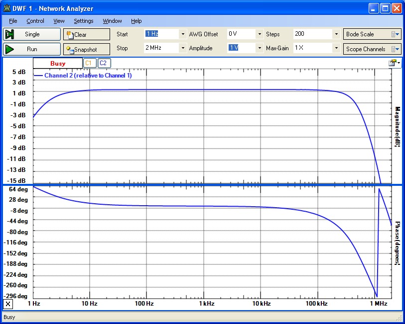
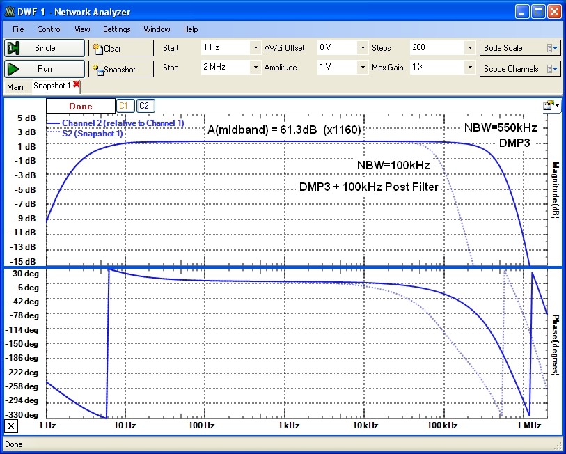
used and is set at maximum gain. Using an input -60dB attenuator, a small-signal Bode plot was generated to determine the mid-band gain and frequency
response for integrated noise amplification purposes for these settings. The plot below was analyzed carefully and the midband gain was 61.3dB (x1160) and the -3dB frequency was
500kHz. The falloff is approximately a 2nd order pole rolloff (40dB/decade). For this type of rolloff, the equivalent sharp-cutoff "noise bandwidth" for total
integrated rms noise is about 1.1f-3dB or 550kHz. By adding a 2nd order Butterworth post-filter (see below), the noise bandwidth can be switched
to 100kHz:
It is important to understand how the preamplifier input and output RC filtering might affect this measurement bandwidth. In this setup, a plug used with
the balanced input reduces the input to single-ended with an input resistance of 100kΩ in parallel with about 50pF capacitance (from schematic diagram). However, the circuit
to be measured (DUT) has an output resistance of at most 100ohm typically which shunts the higher input resistance. In addition, a 2' coax cable with a
capacitance of 60pF was used between DUT and the DMP3. This creates an input low-pass pole with frequency no lower than 100ohm&110pF or 14MHz.
Therefore this input pole for this setup does not affect the measurement bandwidth significantly.
Similarly, the output resistance of the DMP3 final stage is 470ohm. Again the DMP3 output is connected to the scope with a 2' coax cable and the input
capacitance of the scope is 25pF. Therefore the output pole filter frequency is 4MHz, again well beyond the measured "noise bandwith" of 550kHz.
Typical Measurements
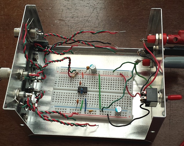
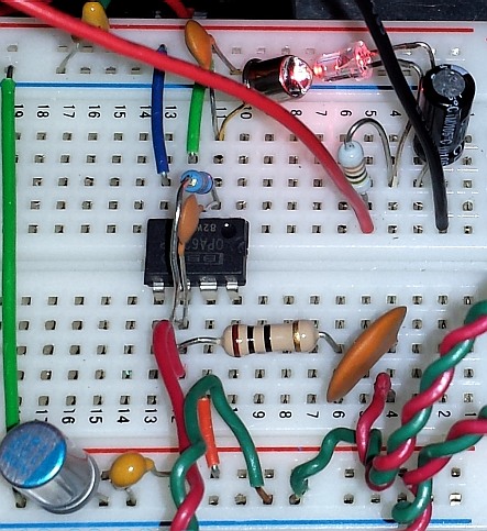
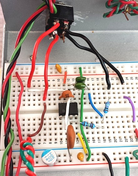
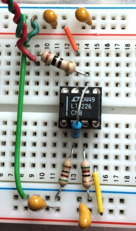
The circuit to be measured was arranged on a small protoboard, with suitable decoupling capacitors, in a shielded box with a separate split battery power supply.
With careful layout, prototyping and testing this way is useful for circuit measurements up to about 20MHz. The total output noise measurements will obviously
depend on the type of circuit and device(s) used in the circuit. Depending on the circuit, the various noise sources (resistor thermal noise, op-amp voltage noise <en>
and current noise <in> etc.)
will be "amplified" in different ways with different spectral profiles (see final paragraph):
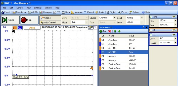
With the shielded box connected to the DMP preamp as described above (but power turned off to the DUT) , the measured rms output noise floor for the setup was ~ 2.0 mV
corresponding to an effective DMP3-input total noise voltage (in the 550kHz noise bandwidth) of 2.0/1160 = 1.7µV, slightly higher than the noise voltage
measured with the scope disconnected completely. Therefore, this configuration can be used to measure DUT total output noise voltages in this bandwidth down to
about 5µV without this background noise floor affecting the results significantly:
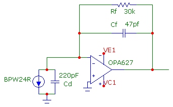
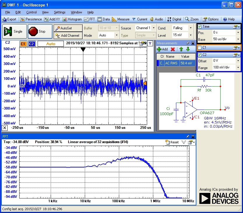
Noise measurement results are shown below for the following basic transimpedance photodiode circuit with a 16MHz OPA627 op-amp. The BPW24R Si PIN photodiode has a bandwidth
of about 40MHz (when reverse biased) with a zero-bias capacitance of about 11pF. The extra 220pF shunt capacitance was added to conveniently study effects such as circuit stability
dependence on photodiode capacitance:
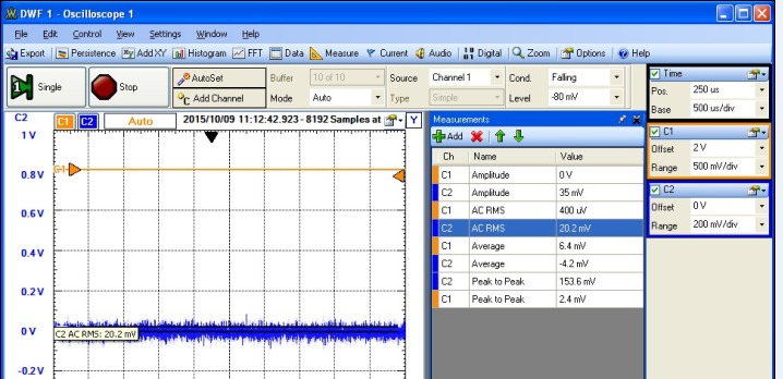
With the photodiode in the dark, the scope noise voltage was 20mV corresponding to a total output noise voltage for the transimpedance circuit of 20.2/1160 = 17µV
in good agreement with the 20µV integrated total output noise calculated for this circuit in a 550kHz noise bandwidth. The total output noise for this circuit in this
bandwidth is
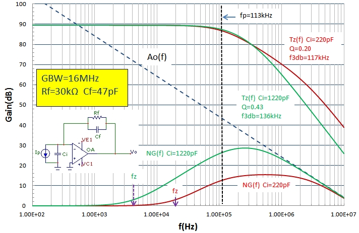
dominated by the amplified en voltage noise of the OPA627 (4.5nV/√Hz). Note that the transimpedance signal bandwidth of 117kHz is somewhat higher
than the pole frequency Rf||Cf of 113kHz as expected for this second-order circuit. Also the en voltage noise continues to be amplified well beyond
this transimpedance "signal bandwidth" frequency as discussed below in a simulation and demonstrated in an FFT measurement:
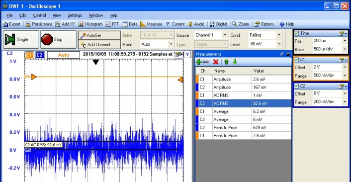
Increasing the total shunt capacitance across the photodiode to 1220pF causes the well-known increased noise-gain amplification for en with
the output voltage noise of the transimpedance circuit increasing to 76.4/1160 = 66µV, in reasonable agreement with the calculated value of 78µV.
Note also (see graph below) that the transimpedance signal bandwidth has increased to 136kHz due to increased frequency "peaking" in the circuit
while the pole formed by Cf||Rf remains at 113kHz. Increasing Cd leads to a higher Q (quality factor) of 0.43 for this "resonant" circuit,
double that of the circuit with Cd=220pF:

Finally, the photodiode was illuminated with an LED. The LED was powered by a separate battery power supply and filtered. An output DC level of 2.88V was measured
corresponding to a photocurrent of 96µA through a 30kΩ feedback resistance. For this measurement, Cd=220pF as for the first meaurement
above:
In this case, the transimpedance circuit output noise of 92.6/1160=80µV is dominated by the photocurrent shot-noise, in reasonable agreement
with the calculated total noise of 68µV.
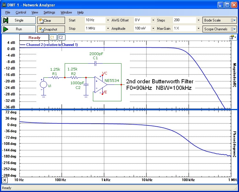
100kHz Butterworth Post-Filter
To narrow the noise measurement bandwidth to approximately 100kHz, a 2nd order Butterworth filter can be added to the OUTPUT of the high-gain DMP3 preamplifier. Since essentially all
the noise and gain are from the DMP3, a very-low noise op-amp is not required for the post-filter. A Butterworth post-filter, using an NE5534 op-amp was designed and built with a F0 (f-3db)
bandwidth of 90kHz. For a 2nd order filter, the corresponding effective noise bandwidth (for an input noise distribution that is frequency independent) is 1.111*F0 = 100kHz.
The noise contribution from the post-filter circuit alone was measured by using it at the INPUT of the DMP3 resulting in an amplified output noise voltage of 7.5mV corresponding to a post-amp output
noise voltage of 7.5/1160 = 6.5µV, completely negligible compared to the DMP+scope background noise floor of about 2mV:
The Butterworth circuit design above assumes an ideal voltage source with zero resistance. However, the output of the DMP3 has a 470Ω series resistance from the
final op-amp output stage. Therefore, to maintain the proper Butterworth filter design when used at the DMP3 output, the input resistor of the Butterworth filter must
be lowered to (1250-470) = 780Ω. The response of the combined system DMP3 + 90kHz post-filter is shown below along with the response without
the filter. Noise measurements of the sample circuit above, are consistent with the calculated
total noise for the smaller 100kHz noise bandwidth. For a simplified
assumption of frequency-independent noise spectral density and noise amplification, and with the total noise scaling as √NBW, one expects the noise for
the 550kHz filtering to be about ~ 2.35x higher than the 100kHz filtered value. However, more accurate estimates of the
total output noise must take into account that
the different noise sources can be amplified with different spectral profiles:
A convenient switching arrangement was used enable/bypass the 100kHz post-filter circuit, as shown below:
How Noise Sources are Amplified
The total measured output noise of a circuit consists of noise contributions from different circuit components, which may be amplified with different
spectral profiles. For example, the basic transimpedance circuit above has output voltage noise contributions from:
- thermal noise of Rf,
- op-amp current noise <in>
- op-amp voltage noise <en>
- signal photocurrent shot noise
For this circuit, each noise source will experience a frequency-dependent amplification transfer function to the corresponding output voltage,
and these noise sources will typically sum as independent noise sources (noise powers add linearly). It is fairly easy to show that for this circuit, the
thermal noise, op-amp current noise and photocurrent shot noise are amplified identically, with the gain profile being identical to that of the transimpedance
function Tz(f) which essentially "filters" these noise sources approximately to the -3db bandwidth of the Tz(f) function.
Therefore the total output noise, up to some finite frequency Fmax, will be a power-summation up to Fmax, weighted by the Tz(f) function, and the shape of
the Tz(f) function will change as the component values change.
The amplification of the op-amp voltage noise <en> is interesting and different in that it experiences an enhanced gain feature (or plateauing effect) arising from the zero
formed by Rf with Ci in the noise-gain function NG(f). This enhanced gain for <en> in transimpedance circuits is particularly evident for higher values of Ci
as is demonstrated below in the FFT noise plot.
To demonstrate the gain profiles, the plots below which don't include the post-filtering used in the measurements, are accurate simulations of the transimpedance functions Tz(f) (actually |Tz(f)|), and noise gain functions |NG(f)| for the circuit
measured above for two different Ci values of 220pF and 1220pF. For this circuit, it can be shown that the TOTAL (integrated over ALL frequency, Fmax-->infinity) output noise due to Rf, <in> and
signal shot noise are independent of Ci (for fixed Rf, Cf and GBW), even though the Tz(f) transimpedance function
changes shape as shown. (This is NOT true for the cumulative total noise for these sources up to some arbitrary finite frequency Fmax).
However as Ci is increased, the total amplified op-amp voltage noise <en> increases greatly as shown, eventually being attenuated by the finite GBW rolloff of
the op-amp. It is for this reason that in transimpedance circuits,
particularly with higher Rf values, it is important to choose an op-amp with very low voltage noise <en> and minimize Ci if possible:
FFT and Noise Spectral Power
The two example below demonstrates continuous noise spectra for two different circuits and how to renormalize an FFT plot of a noise spectrum to a conventional noise power spectrum (in µV/√Hz or equivalent
dBV/√Hz).
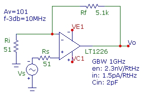
The first example uses a wide band LT1226 op-amp in a standard NI amplifier configuration with an Av=101 (40dB). This circuit is identical to that
presented in the LT1226 spec. sheet as a photodiode amplifier which states a BW of 15MHz. The measured circuit BW here is smaller because of the +/-6V supply used:
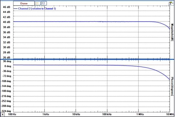
The frequency response of this circuit is shown below with an f-3db of 10MHz:
The total output rms noise voltage and FFT spectrum is shown below, using the DMP3 amplifier configuration described above with a noise-bandwidth filtering set at 550kHz.
Assuming the spectral noise density functions for en, in and thermal noise of Rf are frequency independent (except for low frequency 1/F noise), the output spectral
noise density will be constant with frequency over the full bandwidth of this amplifier and will roll-off as the circuit gain above 10MHz. Since the DMP3 amplifier circuit
post-filters noise with an effective NBW of 550kHz, the amplified output spectral noise will be uniform below this NBW. This is demonstrated in the FFT spectrum below where
the rolloff around 550kHz is evident:
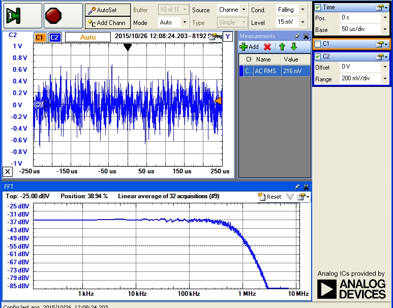
The scope real-time display measurement shows an amplified total noise within this NBW of 216mVrms or -13.3dBV. Since the DMP3 midband circuit gain is 1160,
the LT1226 amplifier output noise voltage is 216mV/1160 = 186µV or -74.6dBV.
This compares well with the calculated total output noise in this NBW of 197µV. This noise is dominated by amplified en noise.
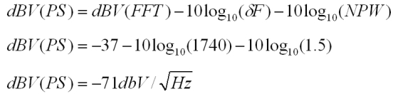
The FFT plot shows a noise level of -37dBV. This refers to the noise within the frequency bin of the FFT sampling and is further increased by filter shape used in the
FFT sampling. To scale the FFT vertical scale to the more conventional power spectral density PS units µV/√Hz, the FFT scale is adjusted for the frequency-bin size δF
and a correction factor for the "noise power bandwidth" NPW of the sample window shape is required. The plot above has taken with a Hann sampling window and δF=1.74kHz
(for the 50us/div used). The Hann sample window has a noise-broadening factor of 1.5. Therefore, applying this normalization for bin size and correcting for the Hann window we have:
To verify consistency, in the passband of the circuit, the op-amp input noise voltage en is amplified with a gain of 101 by the LT1226 circuit and the gain of the post-amp is 1160.
Therefore the total output spectral density is:
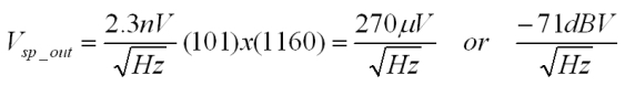
in agreement with the FFT converted value.
Note that in this NI amplifier example, the spectral noise density is fairly flat until the filter rolloff. There is no noise-gain peaking as is evident from the frequency
response plot. This is because the capacitance at the INV op-amp input is fairly low and the resistance to ground there is small as is usually the case for standard
NI voltage amplifiers. In this case, all noise sources (thermal, in and en) are amplified uniformly and are rolled off exactly as the Vs gain function, which in this case
is identical to the noise-gain function.
The second example using the transimpedance circuit above but with Cd=1000pF demonstrates a nonuniform spectral noise pattern clearly showing a
transition from Rf thermal noise domination, transitioning to en dominated noise beyond about 20kHz (see simulation plots above for comparison).
Note that the final measured noise-rolloff is faster than in the simulation above because of the 550kHz post-filter.
Again, it is easy to verify that the FFT value of -58dBV below 10kHz exactly corresponds (after the conversion) to the spectral noise density expected
for a 30kΩ resistor. The thermal noise current of Rf is amplified exactly as the Tz(f) function and rolls off at about 120kHz following the Tz(f) gain as discussed above.
Note that the spectral noise increases beyond this point to over 500kHz! This is because the en source experiences strong spectral noise-gain peaking resulting
from the zero formed by Rf||Ci at lower frequency.
The peak FFT noise value at 300kHz, dominated by amplified en and about 12dB higher than the Rf thermal noise value, agrees with the expected amplified value of en as predicted in the simulation above:
Summary
The system described above provides total integrated noise measurements in a noise bandwidth of 3Hz to 550kHz, and 100kHz.
Circuits with output noise levels of around 5µV or higher can be measured with an estimated accuracy of about 15%.