
Transimpedance Noise Calculation
Aug 05, 2012
This note provides an accurate method for calculating the output voltage noise of the transimpedance circuit shown below:

For the circuit shown, the contributing noise sources are :
- thermal noise of feedback resistance Rf (assuming Ri >> Rf)
- op-amp input current noise in
- op-amp input voltage noise en
in is the spectral current-noise density in units of pA/√Hz or fA/√Hz with a typical value for a FET-input op-amp being ~ 5 fA/√Hz.
en is the spectral voltage-noise density in units of nV/√Hz with a typical value for a "low voltage noise" op-amp being 4 nV/√Hz.
It will be assumed here that these spectral noise densities are constant in frequency (i.e. low frequency 1/F noise is not included).
A simplified view of the total output voltage noise assumes the same noise bandwidth NBW for each of the contributing noise sources. For a single-pole noise filter,
the NBW = NBWsp = π/2xf3db = 1.571xf3db where for a simple RC filter, f3db = 1/(2πRC). In this simplified view, the total RMS output voltage noise for the transimpedance
circuit above is:

This simplified estimate, while sufficient for some circuits, is not accurate for the transimpedance circuit above for two reasons. First, the transimpedance circuit response is
NOT described by a single-pole output filter response but instead is a 2nd order transfer response which can show transimpedance response peaking and a faster response
rolloff than the single-pole case. Second, and more subtly, the input voltage noise contribution from en is amplified by a frequency-varying gain profile (the "noise gain")
which shows a "gain peaking" effect than can lead to unexpectedly high output noise levels compared to the simplified estimate below. This gain peaking results
from the pole in the feedback network formed by Rf and the total input capacitance Ci.
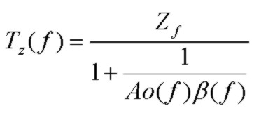
To calculate the correct output noise-voltage for this circuit, the full transimpedance transfer function Tz(f) and the full noise-gain function NG(f) as well as
the finite GWB rolloff of the op-amp must be included in the calculation. Tz(f) includes the effect of the
complex feedback network comprising of Rf, Cf and Ci and the op-amp open-loop gain profile of the op-amp Ao(f) . Ao(f) is assumed here to be described
by a single-pole response. In this case, Tz(f) is a 2nd order transfer function with well known properties identical to those of the passive
series LCR circuit with output taken across C:
The total output voltage noise, obtained by integrating the spectral noise power over all frequency is then given by:

where the noise-gain function is:

Note that poles/zeros in the noise-gain function correspond to zeros/poles in the feedback factor β respectively.
Both the thermal noise and input current-noise terms are "amplified" to output voltage noise terms in exactly the same way as the transimpedance input (current) signal.
However the voltage noise term is seen to have additional gain, simply arising from the zero effect. In fact, the voltage noise is amplified with exactly the same
gain profile as a signal in a NON-INVERTING voltage amplifier would be, i.e. by the "noise gain" or 1/β(f).
The corresponding spectral output power density, in units of V^2/Hz, is then given by:

The simulation plot below shows the output spectral voltage noise (using the parameters for the example given below). At low frequencies, the thermal noise voltage of Rf
is dominant with a value of 28.3 nV/Sqrt(Hz) corresponding to a 50kohm resistor, dominating the low frequency op-amp voltage noise of 6 nV/Sqrt(Hz).
However, as the f3db bandwidth is approached in the vicinity of Fp, a substantial increase of this noise contribution appears as the thermal noise contribution is being rolled-off by
the transimpedance pole response. (The op-amp current noise in this example is negligible).
Eventually, the en noise contribution is itself rolled off by the Ao(f) response which describes the GBW limit of the op-amp itself.
The total output voltage noise is simply the square root of the square sum of the plots over frequency which is expressed in the formulae presented above. (The cumulative
output voltage noise which integrates the noise up to frequency f is shown below in the example section ).
It should be noted that indeed the output noise spectral shape for both the Rf and in contributions can also show some peaking. This is because the thermal and current noise sources
have exactly the same gaining effect as the Tz(f) transfer function and for Q values higher than the maximally flat value of 0.7071 the Tz(f) response shows peaking which means the Rf thermal
and current noise sources will be subject to spectral noise-peaking in the output noise as well:

The total output noise expression above can be transformed into an expression for for concrete integration:

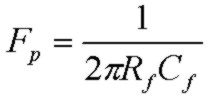
where GBW is the gain-bandwidth product of the op-amp (or unity gain frequency), F0 is the "natural resonant frequency" of the transimpedance circuit and Q is the quality factor:


where the zero and pole frequencies of the noise gain, Fz and Fp are:

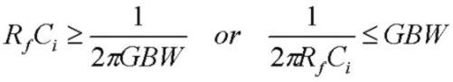
The exact transimpedance f3db bandwidth is defined by:

and is given by:

Note that the f3db bandwidth will vary from below F0 to above F0 depending on the Q value of the circuit which is typically adjusted with Cf.
The condition f3db = F0 is only true for the "maximally flat" frequency response condition of Q = 1/√2. Also, note that while the pole frequency Fp is typically
adjusted (via Cf) to control stability with compensation, the pole frequency is NOT generally equal to the f3db bandwidth in the transimpedance 2nd order transfer function.
However, in the heavily damped limit, Q << 1 where the feedback network pole Fp dominantly controls the transimpedance bandwidth, f3db approaches Fp as expected.
The limiting results are:

The output noise expression contains two integrals:
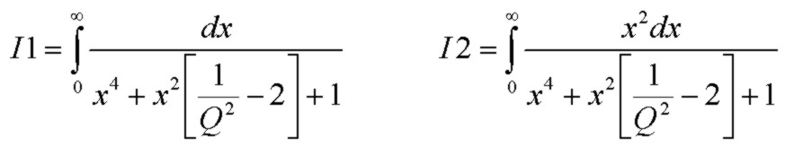
Evaluation of these two integrals interestingly yields exactly the same simple result, namely:

which simplifies the total noise expression to:
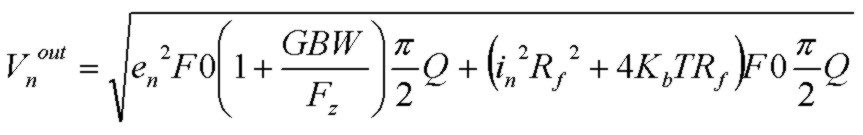
or, introducing "effective noise bandwidths":

It can be easily seen by inspection that the total output voltage noise can be viewed as two contributions with different effective noise bandwidths which
depend on the circuit component values and which account for the full transimpedance response and noise-gain peaking effects:
- the en voltage noise experiences an EFFECTIVE noise bandwidth of NBWen = F0(1 + GBW/Fz)π/2 Q
- the thermal and current noise sources experience an EFFECTIVE noise bandwidth of NBWin_th = F0π/2 Q
Calculating The Noise
Using the above expressions, it is easy to calculate accurately the total voltage noise output for the transimpedance circuit above. The steps are:
- Specify the parameter values which describes the op-amp circuit: GBW, en, in, Rf, Cf, Ci
- Using these values, compute the zero frequency Fz and the resonant frequency F0 using the equations above
- Using these values and the F0 value, compute the Q value for the circuit using the equation above
- Compute the effective noise bandwidths and substitute into the final total voltage noise equation above, using the op-amp en and in noise densities and Rf value
Example:
GBW = 19 MHz en = 6 nV/√Hz in = 2fA/√Hz
Rf = 50kohm
Cf = 2.6 pF
Ci = 20 pF
Q = 0.703
Fz = 141. kHz
Fp = 1.22 MHz
F0 = 1.64 MHz
f3db = 1.63 MHz
NBWen = 246 MHz
NBWin_th = 1.81 MHz
Ven = 94 uV
Vth = 38 uV
Vin = 0.13 uV
Vtotal = 101 uV
This example has a Q value close to the "maximally flat" value of Q = 0.7071.
Note that the effective noise bandwidth for the input voltage noise en is rather large at 246 MHz. This is a consequence of how
the effective noise bandwidth is defined and indicates a significant amount of voltage noise gain peaking, equivalent en noise amplification
extending well beyond the useful f3db signal bandwidth of 1.63 MHz. In this example, the amplifier voltage noise dominates the total output noise.
The calculations presented above are the full output noise voltage values, integrated to infinite frequency. The cumulative noise plots below, which are
obtained by integrating the output voltage noise expression out to a finite frequency f, for the same
example, shows how the en term shows a steep increase, eventually dominating the thermal noise contribution. Notice that the en contribution
extends well beyond the useful transimpedance (signal) f3db frequency of 1.6 MHz:

Techniques for reducing the extent of this en noise-gain peaking with various noise post-filtering approaches are discussed in J. Graeme Photodiode Amplifiers.
The calculator below facilitates computing the voltage noise properties discussed above. Enter the data in the first two rows. Click Get Parameters to calculate
properties in the remaining rows.
For convenience, 3 special buttons are provided which automatically calculate the required exact Cf value (given GBW, Rf and Ci) and all
other parameters for the 3 useful cases:
- Q = 0.50 the critically damped case; no peaking in frequency response and no overshoot in pulse response
- Q = 1/√2 the maximally flat case; maximally flat frequency repsonse with 4% overshoot in pulse response
- Q = 1.00 the "45deg PM" case; 15% peaking in frequency response with 16% overshoot in pulse response
An enhanced version of this calculator is also available separately and also with a minimal interface.
Note on Special Conditions:
Depending on the component values of Rf, Ci and GBW,
a solution for Cf
for underdamped responses, such as the maximally flat condition Q=1/√2 or the popular Q=1.0 case may not be possible.
This may occur for small values of Rf or Ci or GBW. (However, a Cf solution for the critically damped case Q = 0.5 will always be possible).
For the "maximally flat" case with Q = 1/√2, a Cf solution will only be possible under this condition:

For the common case with Q = 1.0, a Cf solution will only be possible under this condition:
In both cases, this means that the zero frequency of the noise gain (or equivalently the pole frequency of the feedback factor β(f)) must be comparable to or less the op-amp GBW for a
Cf solutions with these Q values to exist. This condition will NOT be satisfied if the zero and pole frequencies of the noise-gain are considerably higher than the op-amp GBW.
In that case, the transimpedance f3db bandwidth will simply be controlled by the op-amp open-loop rolloff and f3db will be comparable to the op-amp GBW. Under this condition,
the circuit will typically have a Q value < 0.5 with Cf set to zero (or some nominally small stray value such as 0.3 pF)
and there will be negligible noise-gain peaking in the pass-band of the transimpedance response.
The circuit will have considerable phase margin and will be stable so that no compensation capacitance Cf will be required. Of course Cf could be added to reduce f3db and total
output noise.
Comparison With Approximate Methods
The analysis above for the total output noise voltage is exact within the limitations of the model used. It is interesting to compare the results above with an
alternate method of "segmented calculation". The segmented approach provides a more intuitive view of the various contributing sections (in frequency) to
the total en noise contribution. This is useful for assisting with more advanced methods in optimizing the noise using additional circuit noise-filtering techniques.
In the segmented approach for calculating the en contribution, each region of the noise-gain is treated
separately between different logical frequency segments as described in J. Graeme Photodiode Amplifiers p. 95-102.
The results of this segmented approach as applied to the specific example above are:
- Eno1 (1/F): 0.18 uV
- Eno2 (flat section up to Fz): 2.3 uV
- Eno3 (increasing section from Fz to Fp): 33.3 uV
- Eno4 (plateau section from Fp to NG-Ao(f) intersection: 51.1 uV
- En05 (Ao(f) rolloff contribution): 77.1 uV
- Enoe RMS total for all en parts: 98.3 uV
- En_thermalRF: 39.2 uV
- Eno_ie: 0.14 uV
- Eno_total: 106 uV
Comparing with the above exact analysis, although the results are quite close, the segmented method slightly overestimates the contribution from en
due to the bode-like straight-line approximations used in the simplified analysis of the power integration. (98.3uV compared to 94.0uV).
The Rf thermal and ie contributions in Graeme's approach are slightly higher since that approach assumes a single-pole rolloff at Fp for the filtering of these noise-sources
as compared to the exact 2nd order transimpedance response filtering. The segmented estimate predicts a total output noise voltage of 106 uV compared to 101uV for the exact
calculation, a 5% difference which is sufficiently accurate for all applications considering other uncertainties in circuit components.
Definitions
Below is a response plot showing the definitions of the various terms used in transimpedance amplifier analysis. Note that the "natural resonant frequency" F0
is not the same as the intersection frequency Fc of the noise-gain and the open-loop response.
At Fc, the magnitude of the loop gain |Ao(f)/NG(f)| = 1, and the phase PHA(Ao(f)/NG(f)) at Fc is defined as the phase
margin and determines the circuit stability. In the (almost critically) damped example below, the phase margin is a comfortable 76 degrees.
The dashed curve is simply the noise-gain curve but with the pole Fp not included. This graphically defines the natural frequency F0 as the intersection frequency
of this noise-gain curve (due to the Fz effect only) and the op-amp open-loop gain curve which is exactly the geometric mean of Fz and GBW:

References