1.6 MHz Bandwidth Transimpedance Photodiode Amplifier
July 30, 2012
The transimpedance amplifier implemented with an op-amp exhibits an amazing degree of complexity with many performance parameters that need to be
considered depending on the intended application. This note focuses on component selection for low to intermediate bandwidth (say <~ 100 MHz) applications
and discusses stability and noise. Although important, other characteristics such as low frequency 1/F noise, drift and high signal level considerations are not included here.
This article focuses on general discussion rather than attempting to optimize any specific performance parameter.
The example below demonstrates basic design of a 1.6 MHz bandwidth moderate-gain photodiode amplifier implemented with an op-amp transimpedance circuit.
The circuit modelled and tested here uses the
ADA4627-1
19 MHz, Low Noise, Low Bias Current, JFET Op Amp with
noise spectral densities of en ~ 6 nV/Sqrt(Hz) and in ~ 2 fA/Sqrt(Hz) and input capacitances (Cicm ~ 7pF, Cid ~ 8 pF)
The photodiode has a capacitance of 4 pF, typical of small-area moderately high-speed Si
pin photodiodes (e.g. Vishay BPW24R at -5V reverse bias). Assuming an extra 1 pf of
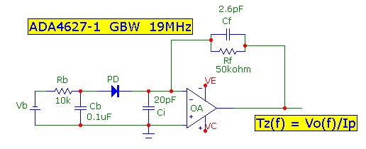
stray and wiring capacitance, the total input capacitance, Ci is taken as 20 pF. A transimpedance value of Rf = 50 kohm is used with a total
shunt capacitance of 2.6 pF across Rf consisting of 0.4 pF stray and a 2.2pF capacitor. The basic transimpedance schematic diagram is shown below:

The photodiode bias circuit components Rb and Cb provide power-supply noise filtering. It is fairly easy to achieve circuit stability and theoretical noise limits using short layout paths and standard
power-supply capacitor decoupling methods and a shielded box:

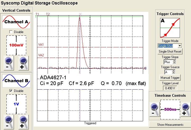
With this op-amp and with the component values shown, the transimpedance 3db bandwidth is calculated to be 1.6 MHz. With the Cf value of 2.6 pF, this corresponds to a maximally flat
transimpedance frequency response with Q = 0.70 and an adequate phase margin of 66 deg at the intersection point of the
noise gain with the open-loop response ensuring stable operation. Design curves are also a very useful graphical aid to quickly determining
circuit component and op-amp selection for a specific application.
Bandwidth Measurement and Q
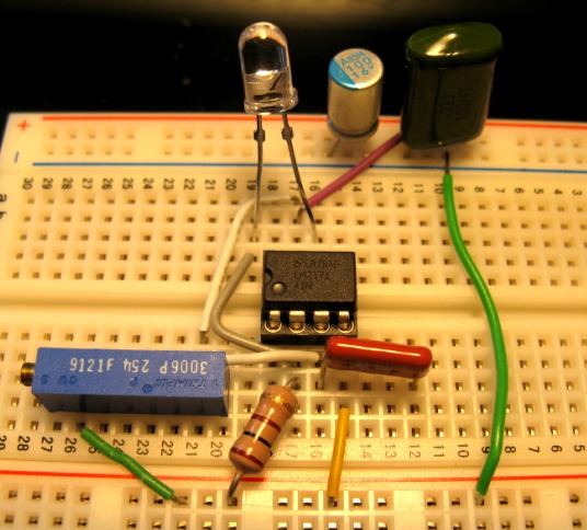
The pulsed response of this circuit using an
infrared LED optical pulse source
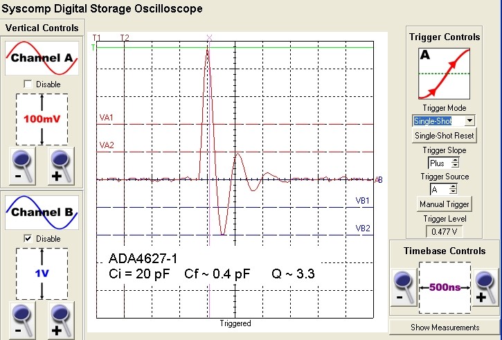
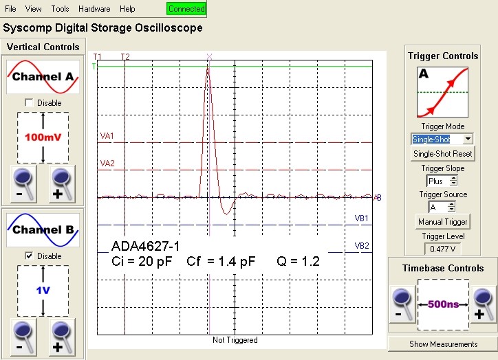
of 30ns duration shows how increasing the feedback capacitance Cf dampens the response (lowers Q):


The 90-10% falltime for the 2.6 pF case is measured to be 240 ns corresponding roughly (assuming a single pole response rolloff) to a f3db BW of 1.5MHz, close to the predicted value of 1.6 MHz.
The section below discusses the more accurate relation between impulse and step response time measurements and f3db in this 2nd order circuit.
Design Synthesis and Q Factor
The transimpedance circuit as modeled above is described by the well known 2nd order transfer function, identical in form and behaviour to the well understood series LRC resonant circuit with output taken
across the capacitor. The quality factor Q is a useful parameter which neatly describes the shape of the transimpedance transfer function including peaking effects. Usually, a design
will target a Q value which provides the greatest bandwidth available but without significant peaking and good stability against oscillation. The typical range :
- Q < 0.50 overdamped response; no temporal overshoot or peaking in frequency
- Q = 0.500 critically damped response; no peaking in the frequency response or pulse response and excellent stability
- Q = 0.7071 the "maximally flat" response; no peaking in frequency and 4% pulse overshoot; good stability with > 60 deg phase margin
- Q = 1.00, a common design target compromise; greater bandwidth; 15% peaking in frequency and 16% pulse overshoot; moderate stability with 45 deg phase margin
- Q > 1.0 underdamped response; large temporal overshoot (ringing) and excessive peaking in the frequency response; low phase margin and instability likely
The other parameter which describes the 2nd order transfer function is the "natural resonant frequency" F0 which is simply the geometric mean of the op-amp GBW product
and the zero frequency Fz of the noise-gain function (or equivalently, the pole frequency of the feedback fraction beta = 1/(noise-gain)) :

A common approximation is to take the transimpedance f3db bandwidth equal to F0. This is exactly true ONLY for the maximally flat condition with Q = 1/Sqrt(2) as indicated below.
The Q value will naturally depend on the op-amp and circuit component values GBW, Rf, Ci and Cf:

One design strategy is to start with given GBW, Rf and Ci values and then determine
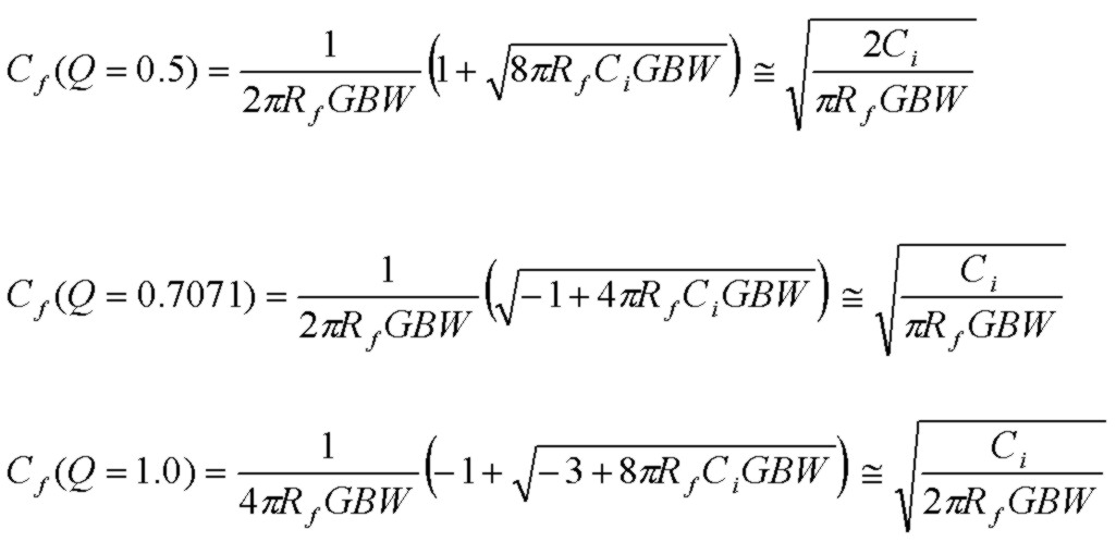
the feedback capacitance value Cf which provides a required value of Q (say somewhere between 0.5 and 1.0). The required value of Cf is given exactly by the solution of a quadratic equation:

Exact Cf results for the most common cases are shown below (and the commonly used approximations in each case which are valid if Cf << Ci). Note that the appoximate Cf values decrease
by Sqrt(2) in each case as the Q value increases:

The 2nd order transfer function can easily be solved for the exact transimpedance f3db bandwidth in terms of the natural frequency F0 and any Q value:

The 3 common cases of interest are:
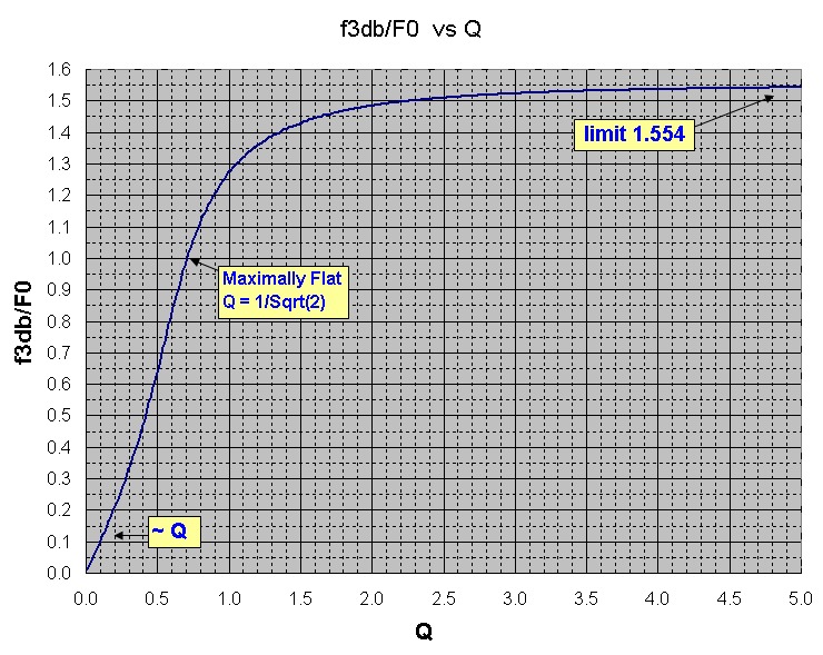
- f3db (Q=0.500) = 0.644F0
- f3db (Q=0.707) = 1.000F0
- f3db (Q=1.000) = 1.272F0
Note that the transimpedance bandwidth is exactly equal to F0 only for Q = 1/Sqrt(2), the maximally flat condition.
The graph below shows the trend. For Q < 0.2, f3db ~ QF0 and for Q >>1, f3db ~ 1.554F0.

Similarly, expressions for the amount of frequency-domain peaking and other parameters are easily determined.
A script calculator solves for all the design and stability parameters of the transimpedance amplifier circuit.
Transimpedance Circuit Noise Discussion
The plots below show the simulated open-loop gain curve |Ao(f)| , transimpedance |Tz(f)| and noise gain |NG(f)| = |1/beta(f)| functions for this op-amp and with the circuit components
shown above.
At low frequencies, the noise-gain is 0 db as expected. The noise-gain zero at 140 kHz arising
from Rf and the total input capacitance and feedback capacitance (Ci +Cf) causes the noise-gain to rise until the noise-gain pole at 1.2 MHz due to Rf and Cf flattens the noise gain curve. The op-amp
input-referred voltage noise en is amplified by this noise-gain profile up to 2.4 MHz and is then rolled off after this intersection point by the op-amp open-loop response limit.
By comparison, the thermal noise of Rf and the op-amp current noise in (flowing through Rf) do NOT experience this same gain-increase, but
are both amplified by exactly the same transfer function as the transimpedance itself and their output noise contributions are rolled-off approximately at the pole frequency 1.2 MHz.
More accurately, it is easy to analytically integrate the noise transfer response for these thermal and current noise sources and find that the
effective NOISE bandwidth applicable to these two noise sources is :
- Q = 0.500 NoiseBW=1.22 x f3db
- Q = 0.707 NoiseBW=1.11 x f3db
- Q = 1.000 NoiseBW=1.24 x f3db
where in each case f3db is the exact 3db bandwidth of the transimpedance response for that value of Q. The maximally flat case for Q = 0.707 achieves the minimum noise bandwidth
(for the thermal and current noise sources only) relative to the transimpedance signal bandwidth f3db. For very heavily damped responses Q << 1, the noise bandwidth tends
to the familiar single pole value of Pi/2xf3db = 1.57f3db.
However the gain experienced by the op-amp voltage noise en can dominate the thermal and current noise sources because (a) the gain increases in value beyond the zero frequency and (b) although
the pole frequency levels off the noise gain, this gain continues at a constant value until rolled off by the op-amps bandwidth limit, and therefore contributes
extra noise beyond the useful transimpedance signal bandwidth limit of approximately the pole
frequency. This implies that for transimpedance amplifiers, an op-amp with just sufficient GBW to achieve the required gain (Rf) and transimpedance bandwidth f3db should be used.
Note that the Tz(f) rolloff is at a rate of 40 db/decade. This is expected since the transimpedance response with a single-pole op-amp is a 2nd order response circuit and therefore
must eventually roll off at this rate:

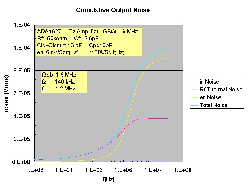
The plots below show the integrated rms cumulative noise terms from each contributing noise source and the total rms-summed output noise voltage with increasing frequency. The Rf thermal noise and op-amp current-noise terms
level off around the pole frequency of 1.2 MHz as expected. However the op-amp voltage-noise contribution en continues to increase for an additional decade in frequency
until the intersection point of the noise-gain and op-amp open loop response beyond which the noise levels off. This extra region of gain for the op-amp noise voltage is "wasted" gain, since the
transimpedance signal gain is rolled off at the lower pole frequency. This extra "peaking gain" region therefore tends to degrade the S/N ratio.
To demonstrate the importance of this, consider the result of using a typical "naive" noise bandwidth for all noise sources as that due to the pole frequency alone and assuming a fixed
0 dB noise gain without peaking.
In this simplified noise estimate (which is approximately correct for the Rf thermal noise and the in noise-current contributions only), the effective noise bandwidth
would be 1.57*Fp = 1.9 MHz (assuming a single-pole rolloff filter at the pole frequency). This naive estimate suggests a total output noise voltage from all contributors of ~ 40 uV, dominated
by thermal noise of Rf.
The true total noise plot below shows that the total output noise voltage is actually ~ 100 uV, 2.5 times higher and dominated by the noise-gain
peaking experienced by the op-amp voltage-noise.

To verify the total output voltage noise of this circuit, two different measurement bandwidths were used:
- a low noise 24bit/96kHz audio sound card with a measured noise bandwidth of 46 kHz was used. A low noise 400 kHz preamplifier with a gain of 200 and input noise level of 1 uV was used.
The transimpedance output measured Vnoise_RMS (46kHz)= 6.3 uV in close agreement with the cumulative noise result for 46 kHz in the simulation.
- a 3 MHz digital oscilloscope (noise BW ~ 5 MHz) with rms voltage measurement was used with a low noise 10 MHz BW preamplifier with a gain of 50 to measure the total transimpedance circuit output noise.
The transimpedance output measured Vnoise_RMS (5 MHz)= 100 uV, in reasonable agreement with the simulated result of 90 uV and dominated in this case by gain peaking of en.
Methods for reducing the effects of the op-amp noise-voltage peaking and thereby reducing overall noise include compensated filtering and post-amp BW filtering of the Tz amp.
These modifications are discussed in Graeme's Photodiode Amplifiers.
Photodiode Dark-Current Noise
The reverse leakage (dark) current of photodiodes contributes shot noise to the transimpedance circuit in exactly the same manner as does the op amp input noise current. Depending on
the photodiode active area, reverse bias voltage and device quality, photodiode dark currents can very over a wide range from hundreds of pA to tens of uA. Usually high speed photodiodes
have small active areas and are characterized by low capacitance and low dark current. Large photodiodes facilitate light-collection but are typically intended for low speed applications. Larger
photodiodes also have significantly lower shunt resistance which contributes thermal noise (in parallel with Rf) and will further increase the noise-gain peaking effect.
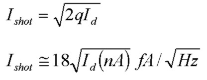
The dark-current shot noise spectral current density, in convenient units is given by:

Small area photodiodes have lower capacitance which is beneficial for lower noise and reverse bias lowers the capacitance further. As a typical example, the Vishay BPW24R at -5V reverse bias has a capacitance of 4 pF.
According to the specifications, the dark current for this photodiode is less than 1 nA at this bias level. Using the expression above and with Id ~ 1 nA, the shot noise density is 18 fA/Sqrt(Hz) or about 9 times higher
than the ADA4627-1 input current noise density. The corresponding output noise voltage contribution from the photodiode shot noise for the 46 kHz BW case and with Rf = 50kohm
is 190 nV and therefore insignificant compared to the 6.3 uV output noise result from the other noise sources. This was verified by noise measurements in this circuit with the photodiode removed from the circuit.
For transimpedance circuits with higher gains however, the photodiode shot noise will become relatively more important as Rf increases. For example, for Id = 1 nA, the photodiode shot noise will be equal to the Rf thermal noise
for Rf ~ 50 Mohm. For Id = 10 nA, the dark-current shot noise will equal the Rf thermal noise at Rf = 5 Mohm. For Id = 100 nA, the dark-current shot noise will equal the Rf thermal noise for Rf = 500 kohm.
The dark currents for two BPW24R pin photodiodes were measured at -5.5V bias using the same transimpedance circuit but with a high transimpedance of Rf = 10Mohm. The output DC offset voltage without
a photodiode connected was measured to be ~ 100 uV in agreement with the output offset expected for this op-amp for Vos and Ib flowing through Rf. The output DC offsets with the reverse-biased photodiodes connected increased to 300 uV and 400 uV. These
correspond to very low photodiode dark currents of 200uV/10Mohm = 20 pA and 30 pA respectively. As a circuit check, a 1N914 Si diode was measured in the same transimpedance circuit to
have a much higher output offset value of 60mV corresponding to a reverse diode leakage current of 6 nA in agreement with the typical spec for this Si diode.
Transimpedance Amplifier Output Offset
Output offset voltage for the transimpedance photodiode amplifier depends on the op-amp input offset voltage Vos, input bias current Ib, and photodiode dark current Id. For the ADA4627-1 op-amp,
the values are Vos = 120 uV and Ib = 5 pA.
The DC noise gain of unity for the transimpedance amplifier determines how the input offset values are amplified. The output offset contribution from the op-amp offset voltage is therfore simply 120 uV.
The very low input bias current of this JFET op-amp ensures very low offset for high Rf values. Ib flowing through Rf contributes an output offset contribution of Ib*Rf which for 50kohm is 0.25 uV. (for Rf = 1Mohm and 10 Mohm, this offset contribution increases
to 5 uV and 50 uV respectively .... usually low enough to ignore). The photodiode dark current also flows through Rf contributing output offset voltage. For Id = 1 nA, the output
offset voltage is 50 uV, increasing to 1 mV for Rf=1Mohm and 10 mV for Rf=10Mohm.
Transimpedance Frequency Response and Time Response
The transimpedance circuit response is characterized by a 2nd order transfer function. Three common ways of measuring the optical bandwidth of the circuit are:
- Small signal frequency response using a frequency-swept modulated optical source with well calibrated response
- Small amplitude impulse response with an optical impulse much shorter than 1/f3db of the transimpedance response
- Step response with a "square" optical pulse with rise/fall time much shorter than 1/f3db of the transimpedance response
It is easy to assemble an optical modulator for frequency response measurements using a high speed high slew-rate op-amp and high-speed LED in a transconductance (voltage to current converter) circuit such as the simple 30 MHz BW modulator shown below:

Circuit 3db bandwidth is often related to the response 10 - 90% risetime τ . For a single pole response characterizing a 1st order network such as a simple RC filter,
the well-known relationship is f3db = 0.35/τ which simple describes a pure exponential decay process. However, for a 2nd order network response such as
the transimpedance circuit, the resonant nature of the response translates into a more complicated relation between risetime and bandwidth. Nevertheless, some sample calculations shown below
illustrate that the single-pole result above is sufficiently accurate for common values of Q (0.5 to 1.0)
Frequency Response
The small signal frequency response is characterized by the transimpedance bandwidth f3db and is obtained with a simple expression given above as a function of F0, the natural resonant frequency of the circuit and the quality factor Q which
both depend on the GBW, Rf, Cf and Ci (and Ri if the input resistance of the op-amp or dynamic resistance of the photodiode are not both very large compared to Rf).
Step Response in Time
Using standard Laplace transform analysis of the 2nd order transfer function, the step response function h(t) for underdamped cases (Q>0.5) is given by (normalized to the DC response value):

where W0 = 2*Pi*F0. Many formalisms use the damping ratio parameter ζ instead of the quality factor Q. They are related by:

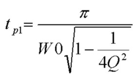
Straightforward analysis shows that the first overshoot peak occurs at a time following the start of the step excitation:

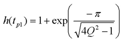
The first overshoot peak ampliltude is given by:

Common values are:
- Q = 1.000 h(tp1) = 1.163 (16% or 1.31 dB overshoot)
- Q = 0.707 h(tp1) = 1.043 (4.3% or 0.37 dB overshoot)
- Q = 0.500 no overshoot (critically damped case)
Numerical evaluation of the 10 - 90% risetime (to the steady state value) for these 3 cases shows that the single-pole result relating 10-19% risetime τ to f3db bandwidth is also a good approximation for the 2nd order transimpedance circuit for
typical values of Q:
- 1st Order f3db = 0.350/τ
- Q = 1.000 f3db = 0.332/τ
- Q = 0.707 f3db = 0.342/τ
- Q = 0.500 f3db = 0.344/τ
- Q < 0.200 f3db ~ 0.350 /τ (overdamped case)
where f3db is related to the resonant frequency W0 = 2*Pi*F0 using the results above for these three values of Q.
Impulse Response in Time
The impulse response for undamped cases Q>=0.5 is given by:

In terms of the measured transimpedance circuit output voltage, feedback resistance and total charge Qtot in Coulombs in the (very short) photocurrent pulse, or incident optical energy Eopt in Joules
and photodetector Responsivity R(λ) in A/W:

The maximum or minimum positions tp in the impulse response can be easily solved as:

Results for the first peak position in time for typical values of Q in terms of the transimpedance 3db bandwidth are:
- Q = 1.000 tp = 0.245/f3db
- Q = 0.707 tp = 0.177/f3db
- Q = 0.500 tp = 0.102/f3db
where f3db is related to the resonant frequency W0 = 2*Pi*F0 using the results above for these three values of Q.
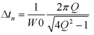
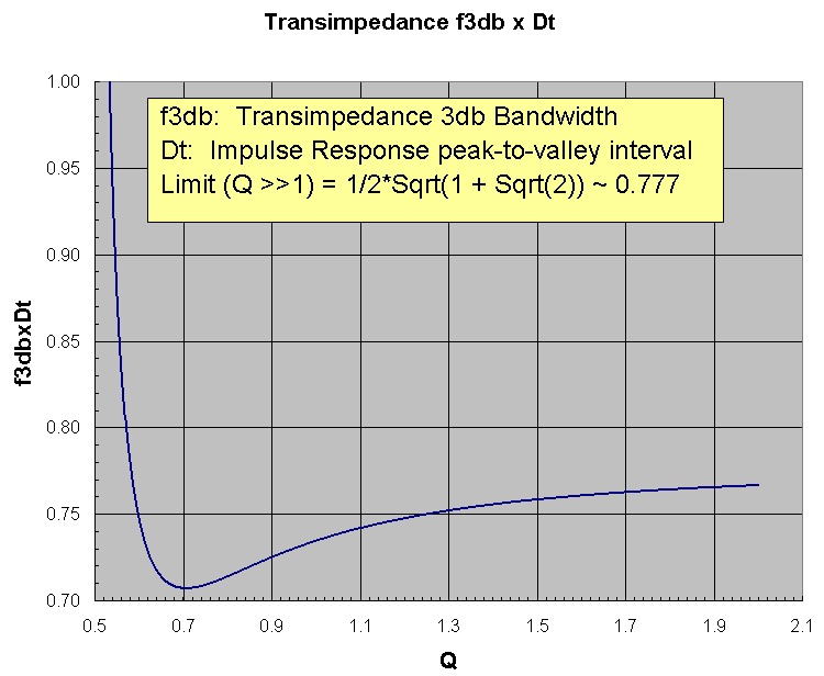
The time interval between any consecutive peak and valley in the impulse response for Q > 0.5 is given by:

and combining with the expression above for f3db in terms of F0:

The plot below shows the dependence with f3db x Δt -> 0.777 as Q becomes considerably underdamped. For the maximally flat response case with
Q=0.707, the factor is also 0.707.

As a sufficiently accurate approximation for any Q > 0.60, f3db ~ 0.75/Δt. From a measurement point of view, this will be the case if
a clear undershoot (minimum) is visible in the transient impulse response.
Measurements of impulse response peak positions therefore can be used to determine the f3db transimpedance bandwidth, for the undamped case of Q >0.5, provided that (a) the optical impulse is much shorter in duration that 1/f3db
and (b) the measurement bandwidth (e.g. oscilloscope) is much higher than f3db.
References

