
Transimpedance Photodiode Amplifier
May 06, 2012
Introduction:
This article discusses basic modeling theory and results for the photodiode transimpedance op-amp circuit.
The exact predicted circuit response, optimum feedback capacitance and phase margin are compared with
commonly used approximate analytical expressions. Calculators are included which (a) accurately calculate the
feedback capacitance required for a stable optimally flat transimpedance response and (b) calculate detailed
transimpedance amplifier properties for arbitrary GBW, Rf, Cf, Ri and Ci parameters.
A specific worked example is included that can be used as a reliable modeling benchmark.
More advanced discussion and design information including noise calculation is available in these articles:
Photodiodes:
The PN junction photodiode is essentially an optical power to electrical current converter. The wavelength
sensitivity of the photodiode depends on the photodiode material (Si, GaAs, Ge etc) with Si photodiodes
being used for visible and near infrared detection. The materials, fabrication design (layer thicknesses etc.)
and wavelength λ largely determine the photodiode Responsivity in units of A/W.
At the most fundamental level, the electronic processes in a semiconductor junction photodiode involve electron and
hole carrier drift and diffusion transport processes. The degree of complexity required in a lumped-circuit element
description of a photodiode depends largely on the intended usage, with speed or bandwidth usually being the
key parameter. Indeed, for speeds in the GHz range or higher, an accurate model requires proper treatment of
the internal junction transit-times and the complexity of the lumped-circuit model increases. For bandwidths
below roughly 100 MHz, the photodiode can be usefully approximated
with an electrical equivalent circuit consisting of an ideal fixed magnitude current source Ip with a shunting
junction capacitance Cp, a shunting junction resistance Rp and an internal series resistance Rs as shown below.
Cp and Rp will be dependent on the reverse bias, if any, applied to the photodiode.
Since the photocurrent generated by a photodiode is a reverse current, the direction of the current source in the equivalent circuit below corresponds
to the orientation of the PN junction in the diagram:

 In this model, the actual frequency response of the photodiode, when terminated into a simple resistive load
is implicitly modeled by its capacitance in parallel with a load resistance. This is a lumped-element simplification of the actual
photodiode transport processes (junction drift and carrier diffusion) which determine the true high frequency
response.
When the photodiode is used with a feedback circuit such as the transimpedance amplifier discussed here, the frequency response will
be determined by the feedback network as well as the amplifier characteristics (GBW etc.).
In this model, the actual frequency response of the photodiode, when terminated into a simple resistive load
is implicitly modeled by its capacitance in parallel with a load resistance. This is a lumped-element simplification of the actual
photodiode transport processes (junction drift and carrier diffusion) which determine the true high frequency
response.
When the photodiode is used with a feedback circuit such as the transimpedance amplifier discussed here, the frequency response will
be determined by the feedback network as well as the amplifier characteristics (GBW etc.).
The photodiode is often reverse-biased to reduce the capacitance Cp, increase linearity particularly at higher optical signal levels, and increase Rp.
For high-quality photodiodes, the leakage current resulting from reverse-bias will be very small (< 1 nA).
The ideal photodiode would have zero Cp and infinite Rp along with the maximal possible responsivity (~ λ(um)/1.24 A/W).
Real photodiodes have characteristics which depend on the intended usage. High speed photodiodes for fibre-optic
systems designed for 100 Mb/s to 10 Gb/s require photodiodes with very low capacitances of <0.5 pF and low reverse leakage current.
For low speed control and monitoring applications where light-collection efficiency and convenience is required, larger area photodiodes
are used with capacitances ranging from 10 pF to 100 pF or higher and lower junction shunt resistances which become important
as well as higher leakage current. The multifaceted design tradeoffs involved in photodiode/op-amp design, with particular emphasis
on low noise for very high sensitivity applications have been discussed in the literature, for example: Photodiode Monitoring with OP AMPS.
This article will focus on photodiodes for intermediate bandwidth applications (BW from 1 MHz - 100 MHz) with Cp ~ 5 pF and Rp ~ 100Mohm.
For the circuit discussed, the photodiode is essentially an ideal current source with a small shunt capacitance, large shunt resistance and low
series resistance. This photodiode capacitance along with the amplifier feedback network will determine the overall amplifier bandwidth and stability. While noise minimization
will be important in low level applications, this article will focus on frequency response and stability and assume higher optical power levels are used.
Transimpedance Amplifier Circuit:
A fairly detailed model for a photodiode coupled to an operational amplifier in the transimpedance circuit configuration is shown below:
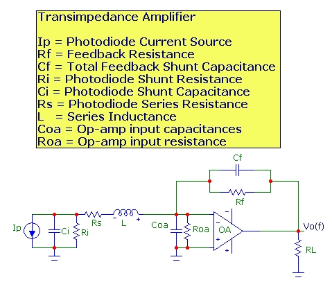
The model for the photodiode includes the effect of series wiring inductance which may be important at higher frequencies depending on the lead length
from the photodiode. As a rough benchmark, for a total lead length of 2cm, the self inductance for 22 AWG (0.064 cm diam) leads is 16 nH. At 100 MHz
the inductive reactance will be 10 ohm and will increase proportionally with frequency.
The op-amp will be modeled as ideal except for a finite gain-bandwidth product with a single low-frequency pole, and input shunt resistance and capacitance as shown.
Since in most cases the series resistance Rs of the photodiode is small (< 10 ohm) and the inductive reactance of L is usually negligible for f < 100 MHz, we will
simplify the circuit by ignoring these. In this case, the shunt resistances and capacitances of the photodiode and op-amp are in parallel and can
be treated as single parameters. This circuit has the nice property that the response has a 2nd order filter-response shape which provides better insight into
the capacitance effects on bandwidth and stability. (The exact transimpedance transfer function for the detailed model is provided in Appendix A below)
The resulting simplified circuit is shown below:
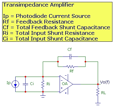
The total input shunt capacitance Ci is the sum of the photodiode capacitance, the input capacitances of the op-amp
and stray layout capacitances.
Op-amp input capacitances vary considerably depending on the type (bipolar, FET input etc.) with values ranging from a few pF to
a few tens of pF. The total feedback network shunt capacitance Cf consists of feedback capacitors explicitly added as
well as parasitic shunt capacitances (which can vary from 0.1 to 0.5 pF depending on the components used).
We will discuss a specific example here with these characteristics:
- Ci = 15 pF (Cd = 5 pF + Camp = 10 pf)
- Cf = design variable
- Ri = 100 Mohm
- Rf = 10kohm
- OpAmp GBW = 100 MHz single pole response over entire open loop gain curve
Transimpedance Amplifier Model:
The operational amplifier is modeled as an ideal voltage-feedback op-amp except for:
- finite GBW with an idealized single pole 6dB/octave rolloff
- finite input capacitances
- finite input resistance
The transimpedance transfer function Tz(s) for the circuit shown above is defined as:
Tz(s) = Vo(s)/Ip = Zf(s) / (1 + 1/(Ao(s)*beta(s)))
where s is the complex radian frequency s = jw = j*2*pi*f
Zf(s) is the frequency dependent feedback network impedance:
Zf(s) = Rf || Cf = Rf / (1+s*Rf*Cf)
Ao(s) is the frequency dependent single pole open loop gain function for the op-amp:
Ao(s) = Ao/(1 + s/wb)
beta is the complex feedback fraction and NoiseGain(s) = 1/beta(s) = (Zf(s) + Zi(s))/Zi(s):
NoiseGain(s) = (Rf + Ri)/Ri *(1 + s*Rf*Ri/(Rf + Ri)*(Cf + Ci))/(1 + s*Rf*Cf)
which for very high Ri which usually applies to high speed photodiode/amplifier designs reduces to:
NoiseGain(s) = (1 + s*Rf*(Cf + Ci))/(1 + s*Rf*Cf)
This noise-gain function has a pole at:
fp = 1/(2*pi*Rf*Cf)
and a zero at:
fz = 1/(2*pi*Rf*Ri/(Rf+Ri)*(Cf + Ci))
or for Ri>>Rf, approximately:
fz = 1/(2*pi*Rf*(Cf + Ci))
In some discussions, the transimpedance amplifier response is simplified to:
Tz(s) ~= Zf(s)
which roughly predicts the high frequency rolloff, but doesn't include feedback phase shift effects which leads to response peaking as will be
demonstrated in the example below.
In an ideal transimpedance amplifier configuration, with negligible Ci and Cf, the transimpedance amplifier 3db bandwidth will be equal
to the unity-gain bandwidth (or GBW) of the operation amplifier, since in this case the noise-gain will be frequency independent and unity. The frequency Fc
at which the noise-gain curve intersects the open-loop op-amp gain curve determines the closed-loop circuit bandwidth. For a realistic circuit, with finite Ci, the noise-gain curve
will have a zero which causes the noise-gain curve to rise with increasing frequency.
This leads to a reduced intersection frequency, a corresponding lower transimpedance bandwidth and the potential for instability and oscillation due to feedback network phase-shift.
The frequency dependent loop gain is defined as Ao(s)*beta(s). The usual condition for sufficient stability against oscillation of an op-amp circuit is
that the phase margin (180 deg + loop gain phase) should be at least 45 deg. at the point Fc where the NoiseGain intersects the op-amp open-loop gain curve, i.e. at |Ao(s)*beta(s)| = 1)
. Note that the loop gain phase is negative and at least -90 deg due to the low frequency pole of Ao(s). Input capacitance Ci will
further reduce the loop gain phase, tending toward the -180 deg instability point, corresponding to 0 deg phase margin.
Using some approximations and realizing that the NoiseGain has one zero at lower frequency and one pole at higher frequency,
the condition for at least 45 deg phase margin can be satisfied by adjusting the feedback shunt capacitance Cf so that the pole fp is placed at the intersection point of the noise-gain and Ao(s).
The resulting approximate expression which is frequently stated is:
Cf_45 = Sqrt(Ci/(2*pi*Rf*GBW))
along with the corresponding 3dB frequency response BW which in this case is just the pole frequency at this value of Cf:
f3dB(Cf_45) = Sqrt(GBW/(2*pi*Rf*Ci))
These expressions are often used as a starting point for design.
Often this value of Cf in fact leads to too much peaking in the frequency response and overshoot in
the transient response. This is due to additional phase shift in real op-amps arising from additional high-frequency poles in the open-loop response.
A more conservative starting point uses the "optimally flat" Cf value, which is approximately 40% higher in value than Cf_45. The "optimally flat" response is discussed in detail below..
Comparison of Model Results:
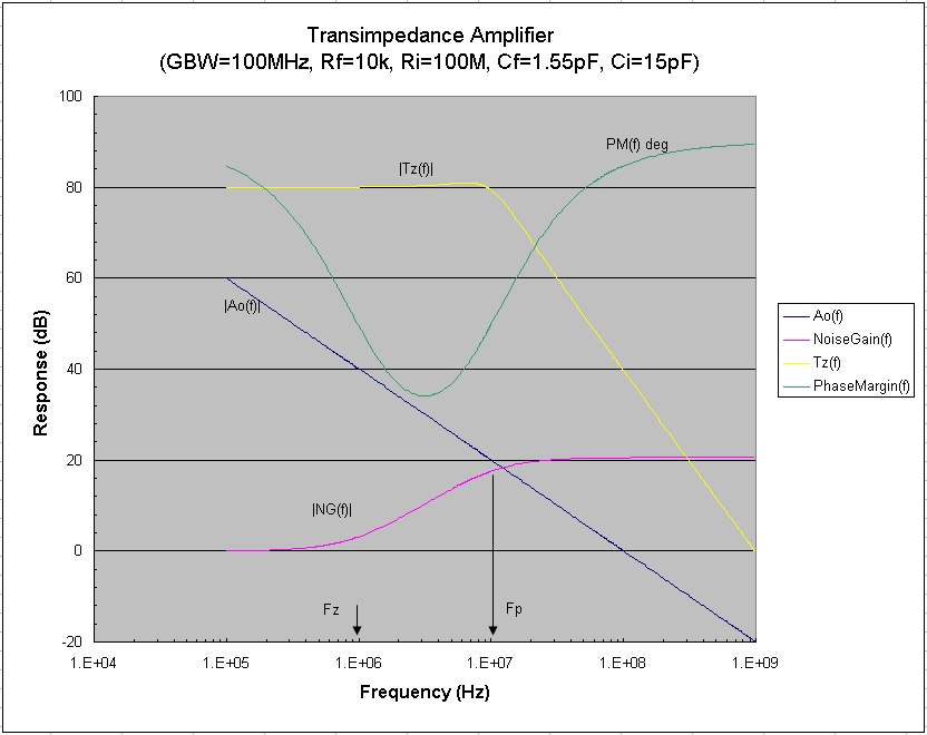
It is interesting to check the accuracy of these expressions for Cf and BW against an exact model calculation.
Using the component values above, the simplified expressions predict:
Cf_45 = 1.55 pF
f3db = 1/(2*Pi*Rf*Cf) = 10.3 MHz
A numerical calculation using the complete transimpedance transfer function and NoiseGain
expressions above and using Cf = 1.55 pf predicts:
Intersection Frequency: f(|Ao(s)beta(s)|=1) = 12.2 MHz
Phase Margin: 55 deg
f3db = 12.2 MHz
Peaking: 0.96 dB peaking at 6.5 MHz
showing that the pole frequency fp (10.3 MHz) is not quite at the intersection point (12.2 MHz) but is lower in frequency, providing more phase margin
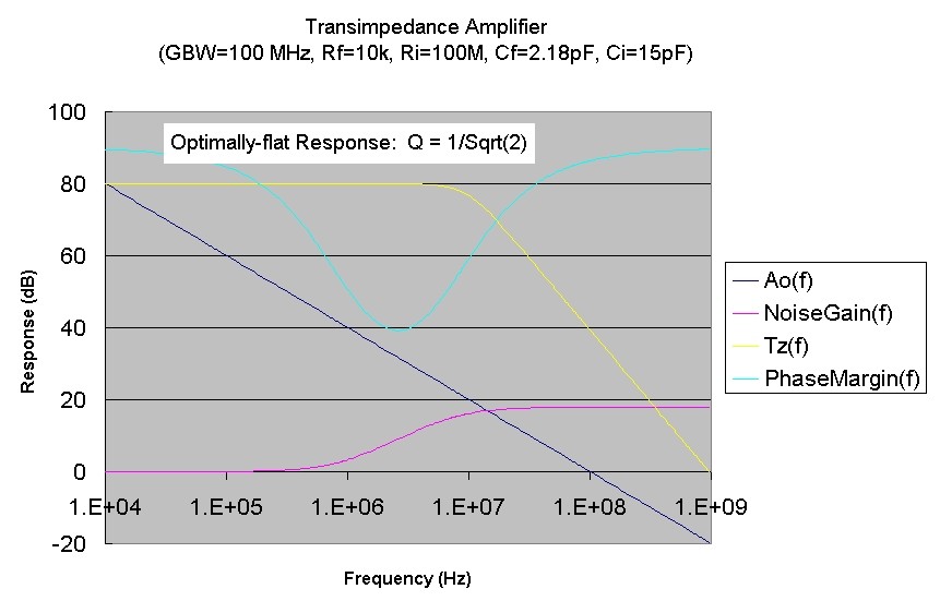
than predicted by the simple expression. Simulation plots showing the magnitudes of the transimpedance, open loop gain and the noise gain in dB
are shown below. While the "phase margin" is strictly defined as the difference between 180 deg and the phase of Ao(s)beta(s) at |Ao(s)beta(s)|=1,
the curve below displays this phase difference at all frequencies :
For comparison, solving the EXACT expression for Cf which places fp at the intersection point yields a Cf = 1.36 pf.
Using this Cf value in the exact calculation predicts:
Intersection Frequency: f(|Ao(s)beta(s)|=1) = 11.7 MHz == fp
Phase Margin: 50 deg
f3db = 12.9 MHz
Peaking: 1.6 dB peaking at 7.4 MHz
demonstrating that even when fp is placed exactly at the intersection point, the phase margin is still greater than 45 deg.
These exact calculations on a fairly basic photodiode/transimpedance amplifier circuit demonstrate that the Cf result obtained
using the well known simplified expressions is a conservative estimate providing somewhat greater phase margin and
actually places the pole frequency below the intersection point of |Ao(s)| and |NoiseGain(s)| or |Ao(s)*beta(s)|=1. Greater phase margin, flatter response and somewhat
lower transimpedance bandwidth is provided by selecting Cf to achieve an "optimally flat" response as discussed in the next section.
Optimally Flat Butterworth Response Cf Value:
The model above uses the simplest possible form for the op-amp open-loop response, i.e. a single-pole model. The value of Cf above which places the feedback
pole at the intersection of the noise-gain with the open-loop response still leads to some response peaking in the frequency response and overshoot in the real time pulse response.
All real op-amps have additional higher frequency poles located near the unity-gain frequency which cause the phase accumulation (due to Ao(s)) to be greater than the -90 deg. value for a single pole.
Generally this will lead to greater peaking. A more appropriate somewhat higher value for Cf (heavier damping) can be chosen. For the single-pole model of Ao(s),
it is interesting and instructive to write the exact transimpedance transfer function, Vo(s)/Ip in a form clearly showing the response as a 2nd order filter response
with parameters wo = 2*Pi*F0 (natural or undamped resonant frequency) and Q (quality factor) which both depend on GBW, Ci, Cf and Rf:
Tz(s) = Vo(s)/Ip = Rf*Ao/(Ao + 1) * wo^2/(s^2 + s*wo/Q + wo^2)
Since this is a 2nd order response, the transimpedance must eventually roll off at a rate of 40 dB/decade, as evident in the |Tz(f)| plot above.
In this model, an "optimally flat" transfer function response is obtained if we choose Q = 1/Sqrt(2) = 0.7071 which leads to a 3dB bandwidth for Tz(s) of exactly F0.
(The less damped Cf_45 case discussed above corresponds approximately to Q = 1.0).
It is easy to solve for the corresponding value of Cf, given GBW, Ci and Rf, by using either a simple iterative approach which converges rapidly, or the
exact quadratic solution for Cf can be used.
Simplified well-known expressions which offer some insight can be easily obtained for Cf and f3db which are sufficiently accurate in most cases of interest assuming Cf < 0.2*Ci.
These simplified equations give Cf results which are somewhat higher than the exact Cf values and f3db values somewhat lower than the exact values:
Cf_flat = Sqrt(Ci/(pi*Rf*GBW))
The optimally flat Cf value is Sqrt(2) times higher than the Cf_45 value above or 2.18 pF in this example. The phase margin is increased to ~ 67 deg.
This "optimally flat" Cf value shows no frequency peaking and leads to a 3dB bandwidth of the transfer function equal to the natural frequency F0:
f3db_flat = F0 = Sqrt(GBW/(2*Pi*Rf*(Cf_flat + Ci)) .
It is noted that f3db_flat is the geometric mean of the noise-gain zero frequency (1/(2*pi*Rf*(Cf + Ci)) and the GBW product (or unity-gain frequency
in the simplified single-pole Ao(s) model used here).
It should be noted that with lower Rf or GBW values, the simple expressions above can differ considerably from the true results.
For example, with GBW=10MHz, Rf=1kohm and Cs=15pf, the simple expressions predict Cf= 22pf and f3db=6.6MHz but the exact results are Cf=15pf and f3db=7.3MHz.
Although for most practical cases of interest (Ci, Rf, GBW values) a solution for Cf exists, it should be noted that for a given target value of Q, there is a minimum value of Ci below which Cf is undefined.
This minimum value (which corresponds to Cf=0) is:
Ci_min = Q^2/(2*pi*Rf*GBW)
which for the optimally flat response case, Q = 1/Sqrt(2) is:
Ci_min = 1/(4*pi*Rf*GBW)
This simply means that for lower values of Ci, this value of Q is not achieveable because the feedback zero fz = 1/(2*pi*Rf*(Ci+Cf), is very close to, or above the unity-gain frequency of the op-amp
so that the feedback network phase shift is negligible and the rolloff is determined by the op-amp single-pole rolloff.
In simple terms, the circuit components for the configuration create a damped response, incompatible with the requested Q value.
The results for the optimally flat response, and the resultant response curves for our sample case are:
Phase Margin: 67deg
f3db = 9.63 MHz
Peaking: no peaking
Transimpedance Calculators:
Two convenient independent script calculators are included below for the transimpedance circuit.
A more general calculator for feeback stability
including results for the noninverting and inverting circuit is available. They can be used to assist with design and analysis of transimpedance circuits, quickly check
dependencies and verify accuracy of the simplified expressions. Since the results of these calculators are exact (within the limits of the model used),
they can be compared to the results of advanced circuit simulation software to verify software accuracy or to determine how important other non-ideal
op-amp characteristics which are included in the software (such as higher-oder internal poles etc.) are in circuit performance.
To summarize, the circuit and op-amp model used for the calculators below are:
- op-amp: finite GBW with single-pole Ao(s); input capacitances (include in Ci); op-amp internal output resistance = 0
- feedback resistance Rf
- feedback total shunt capacitance Cf
- Ri = infinite in first model; Ri = finite in the second model
- input total shunt capacitance Ci at inverting input
The first calculator simply computes the Cf and f3db values for an optimally flat response Q=0.707
given GBW, Rf and Ci (assuming Ri = infinite) using
(a) the simplified expressions above and (b) the exact quadratic solution:
| Cf and f3dB Calculator for Optimally Flat Transimpedance Response |
The second calculator computes detailed and exact transimpedance amplifier properties for given GBW, Rf, Cf, Ri and Ci. (With Ri included, the 2nd order transfer function Tz(s) above
has an identical form with a slightly modified Q value involving Ri||Rf).
- exact transimpedance 3dB bandwidth and Q value
- intersection frequency Fc where |Ao(s)beta(s)|=1 and phase margin
- peaking frequency Fpeak (if defined) and Peaking value in dB
- the noise gain pole fp and zero fz
Apart from parasitic components, probably the total input capacitance Ci will be the least certain property since it depends on the photodiode capacitance
(which is bias dependent), and the various op-amp input capacitance contributions which depend greatly on the op-amp design and which are not always
specified in the manufacturers' specifications.
Remember that lower Q means higher damping which means less peaking in the frequency domain and less overshoot in the time domain but lower transimpedance
bandwidth. Representative values as discussed above are:
- Q>1 significant peaking and overshoot
- Q=1.000 Cf_45
- Q=0.707 optimally flat
- Q=0.500 critically damped
- Q<0.5 no peaking or overshoot
Comparison with LCR Resonant Circuit:
To cast the transimpedance response into a more familiar light, it can be seen that the 2nd order transimpedance transfer function above is identical
in form to that of the well understood simple LCR resonant series circuit with response output taken across the capacitor.
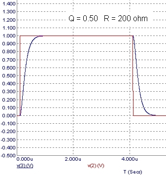
The simple example below shows an "optimally flat" LCR resonant circuit example:
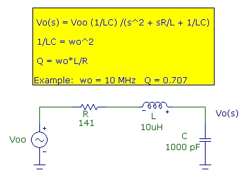
One usually refers to the damping of an LCR circuit in terms of a damping coefficient alpha = R/(2*L) which describes the exponential damping of the transient response.
"Critical" damping occurs for alpha = wo which can be seen corresponds to Q = 0.5. In the example above, critical damping would correspond to R = 200 ohm.
Therefore, the "optimally flat" condition with Q = 0.7071 corresponds to strong but not quite critically damping. The Q=1 case corresponds to R = 100 ohm.
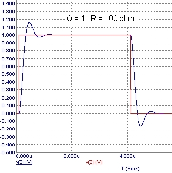
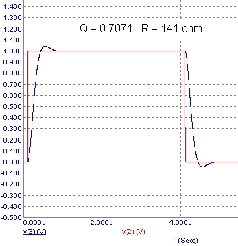
The modeled pulse response for this LCR circuit demonstrates the pulse-overshoot expected:
- Q = 1.0 with 16% overshoot
- Q = 0.7071 with 4% overshoot (optimally flat response)
- Q = 0.5 with 0% overshoot (critically damped)
Examples of Photodiode Transimpedance Amplifier Compensation:
Some simple examples will demonstrate the effects of the feedback compensating capacitor for two quite different op-amps.
A Vishay TSFF5210 high-radiance 870 nm LED was used as the optical source. The LED was driven by a simple 2n2369a avalanche transistor pulse circuit
as shown below:
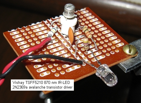
This driver generates short optical pulses with fall-time of about 15 ns, consistent with the 25 MHz BW of this LED. Due to the high
LED drive current, the rise time is shorter at 6 ns, limited by the oscilloscope.
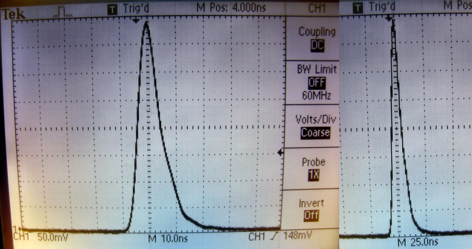
The optical pulse shape is shown below using a Thor Labs PDA10A photodiode with a bandwidth of 150 MHz.
A Tektronix 60 MHz TDS 210 oscilloscope was used for all measurements below.
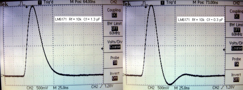
The transimpedance pulse responses using a 50 MHz photodiode and a National LM6171 100 MHz GBW op-amp is shown below.
With a feedback capacitor of 1 pF and about 0.3 pF parasitic capacitance and with Rf = 10kohm, the pulse response shows a smooth fall time of
about 32 ns (11 MHz) demonstrating almost perfect compensation. This is close to the modeled example above.
By comparison, the result with just the 0.3 pF parasitic capacitance demonstrates an undercompensated configuration with
response peaking leading to pulse overshoot/ringing:
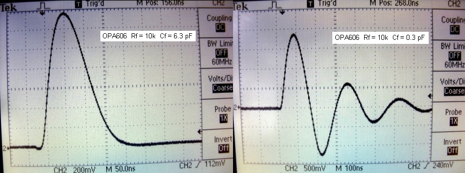
With a much lower bandwidth op-amp, such as the 12 MHz GBW OPA606 op-amp, the lower loop-gain means that for a given nominal
transimpedance gain, a greater compensation capacitor Cf must be used to eliminate gain peaking and pulse-overshoot. This of course
means that the bandwidth will be lower. The results shown below for the OPA606 illustrate this. Again with an Rf of 10k, the feedback capacitor required
to eliminate peaking is about 6 pF with a resultant 3dB bandwidth of about 3 MHz, almost 4 times lower than the bandwidth achievable with the 100 MHz op-amp.
The ringing shown for the Cf ~ 0.3 pF corresponds to a very low phase margin of 25 deg. with an associated transimpedance gain peaking of over 7 dB.
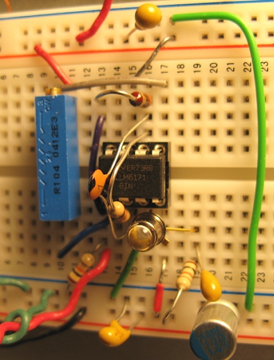
The measured results above were obtained using simple breadboarding as shown below. This works reasonably well, and allows one to quickly
compare active and passive devices and component layout criticality. However one must obviously quantify the parasitic capacitances inherent in
breadboarding. For example, inter-track capacitance can vary from 0.3 pF to over 2 pF which is clearly important in transimpedance circuits.
Nevertheless, it is possible to achieve good results in bandwidths of up to about 50 MHz with some care.
Decompensated op-amps as transimpedance photodiode amplifiers:
It is possible to use op-amps that are not unity-gain stable in transimpedance circuits provided that the noise-gain at the intersection of the noise-gain curve
with the open-loop op-amp gain is greater than the minimum gain specified for the op-amp. For example, the 500 MHz LT1222 op-amp is
specified as being stable in a gain of 10 or greater. The 2 pF input capacitance of the LT1222 is lower than that of the op-amps above, and
with a total input capacitance of about 9 pF and the greater bandwidth, an optimum Cf value of ~ 0.5 pf is found for Rf=10 kohm. With this value, the noise-gain
at crossover is about 14 and the configuration is therefore stable. However this Cf value leads to excessive ringing in this circuit. The ringing can be almost eliminated
by increasing Cf to about 0.9 pF which however reduces the noise-gain at crossover to just over 10. The clean response is shown below:
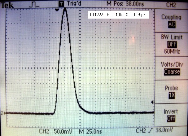
A fall time of about 15 nS or a bandwidth of about 23 MHz is observed as predicted by
the simulation. Since the noise-gain asymptote at high-frequencies is (Cf + Ci)/Cf, this can be used to roughly estimate the noise-gain at the
intersection. This indicates that since Ci is usually considerably greater than Cf, increasing Cf will LOWER the noise-gain at the intersection,
which will eventually move the decompensated op-amp into instability. For the LT1222, a Cf > 1 pF leads to instability and oscillation
is observed.
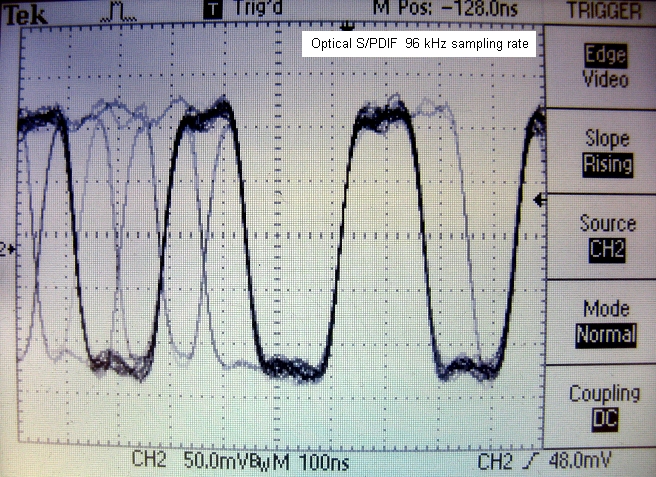
Optical S/PDIF Stream:
Digital audio data streams are encoded using the S/PDIF format (Sony Phillips Data Interchange Format) for transmission electrically or optically.
This format defines a frame of sampled data along with status/copyright information as 64 bits in length and repeated at the audio sampling rate (44.1 kHz
for CD-DA and up to 96 kHz for higher quality audio). For 96 kHz sampling rate, the bit rate is 96kHz * 64 bit = 6,144,000 bps. The encoding
in the data stream defines a ONE bit as making two transitions in the bit interval whereas a ZERO bit has only one transition at the START of the
bit interval. Therefore the ZERO pulse width is about 81.4 ns and a ONE pulse width is 163 ns. Typical optical S/PDIF data streams at the
"digital optical out" interface for comsumer grade products use 650 nm LEDs as sources and have average optical power of about 10 uW or -20 dBm.
The image below shows a monitored S/PDIF 96 kHz data stream, triggered to display both ONE and ZERO
bits. The LM6171 transimpedance amplifier above with Rf=10k was used.
The 11 MHz (32 ns) BW of this photodiode-amplifier combination allows the one bits to just be resolved.
The optical fibre was loosely butt-coupled to the photodiode. At 650 nm the responsivity of
the photodiode is about 0.4 A/W and with an optical coupling efficiency to the detector of about 25%, the photodiode current is ~ 1 uW. With an Rf of 10k,
this translates into 10 mV peak output level. A simple wideband post-amp with Av= 20 (26 dB) was used to raise the signal level to ~ 200 mV as shown:
Appendix A: Transimpedance Transfer Function for Detailed Circuit:
The detailed photodiode-op-amp circuit above including the effect of the photodiode series resistance Rs can be easily analyzed by recognizing that the input network (to the inverting op-amp terminal) can be simplified using a Norton
equivalent circuit with the entire input network replaced by an effective Norton current source Ip_n (which will depend on frequency) and a single Thevenin shunting impedance Zi_ef at the inverting input.
With this circuit reduction, the transfer function (to the output of the op-amp) becomes simply :
Vo(s) = Ip_n*Zf(s) / (1 + 1/(Ao(s)*beta(s)))
where
beta(s) = Zi_ef/(Zi_ef + Zf)
Zf = Rf/(1 + s*Rf*Cf)
The circuit reduction is shown below:
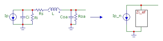
The Thevenin impedance Zi_ef is simply the impedance, looking back (to the left) into the network with Ip open-circuited. With the following convenient impedance combinations defined:
Zi = Ri/(1+s*Ri*Ci) parallel combination of Ri and Ci
Zs = Rs + sL series combination of Rs and L
Zoa = Roa/(1 + s*Roa*Coa) parallel combination of Roa and Coa
we find that the Thevenin effective impedance is:
Zi_ef = Zoa*(Zi + Zs)/(Zoa + Zi + Zs)
and the effective (short-circuit) Norton current is:
Ip_n = Zi/(Zi + Zs)*Ip
Therefore the transimpedance, related to the original (fixed) photodiode current source is:
Tz(s) = Vo(s)/Ip = Zi/(Zi + Zs)*Zf(s) / (1 + 1/(Ao(s)*Zi_ef/(Zi_ef + Zf) ))
This form can be easily calculated and plotted on any scientific calculator with complex math capability. Similar equivalent circuit reduction can be applied to more complex input networks.
References
- Compensating for the Effects of Input Capacitance .., Analog Devices MT-059
- Design Considerations for a Transimpedance Amplifier, National Semiconductor AN-1803
- Texas Instruments: High Speed Analog Design and Applications Seminar
- LMP7717 88 MHz, Precision, Low Noise Op-Amp , National Semiconductor LMP7717 Data Sheet
- Compensate Transimpedance Amplifiers Intuitively, Texas Instruments Application Report SBOA055A
- Understand and apply the transimpedance amplifier, David Westerman, PlanetAnalog Document 2007
- Photodiode Monitoring with OP AMPS, TI Technical Document SBOA035 1995
- Designing Photodiode Amplifier Circuits with OPA128, TI Technical Document SBOA061 1994
- OPA380 Precision High-Speed Transimpedance Amplifier, OPA380 Data Sheet
- OPA656 Wideband, Unity-Gain Stable, FET-Input OpAmp, OPA656 Data Sheet
- IC OP-AMP Cookbook, Walter Jung, 2nd Edn. 1980 SAMS.
- Microelectronic Circuits, A. Sedra and K. Smith, 2nd Edn. Holt, Rinehart and Winston, 1987 p.724