Bias Offset Noise
May 06, 2012
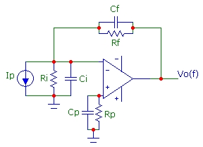 Consider the following transimpedance circuit where Ip could represent the photocurrent of a photodiode.
Ci and Ri are the total input shunt capacitance and resistance at the inverting input.
In the following, it will be assumed that Ri >> Rf which is true in many cases.
It is common practice to use a bias-current compensation resistor Rp ~ Rf to cancel DC output offset errors originating form ib.
However, introducing Rp increases the output noise of the circuit since the thermal noise of Rp experiences the full noise-gain amplification,
including any noise-gain peaking effects originating from the noise-gain zero at Fz = 1/2πRf(Cf+Ci).
(Current noise in also contributes input voltage noise but will be ignored here assuming a FET-input device with extremely low in)
This contrasts with the thermal noise contribution from Rf which does NOT experience
the noise-gain peaking effect with the thermal noise of Rf merely being rolled-off by the feedback pole, augmented by the op-amp intrinsic bandwidth roll-off.
A common solution for reducing the thermal noise contribution of Rp is to bypass the offset resistor Rp using a shunt capacitance Cp
thereby creating an input low-pass filter (or pole) for the thermal noise of Rp. To ensure that the thermal noise of Rp is significantly lower than that of Rf, Cp
should be chosen so that the pole frequency 1/2πRpCp is considerably lower in frequency than the zero frequency Fz of the noise gain. In fact if this pole frequency were chosen to be
exactly equal to the noise-gain zero frequency, we have effectively a compensated divider for the gain experienced by the thermal noise of Rp, since the increasing gain
from the noise-gain zero would exactly cancel the input rolloff of RpCp. For this (incorrect) choise of Cp, in fact the output thermal noise due to Rf would
be exactly the same as the output thermal noise from Rp (with Rf = Rp):
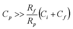
Therefore a higher value of input shunt capacitance must be chosen to roll-off the input thermal noise voltage well BELOW the noise-gain zero frequency:

The example below shows how the contribution to total output voltage noise changes as Cp is increased. The compensated divider condition
is at Cp = 22.6 pF for this particular circuit and op-amp. Choosing Cp ~ 10x this value will ensure that the thermal noise of Rp is neglibible.
Example
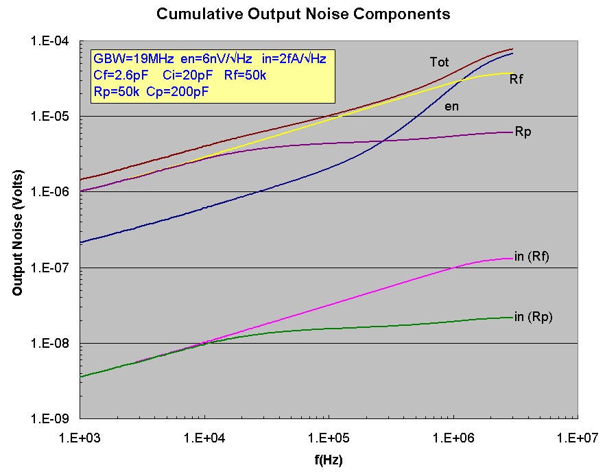
The table below shows the transimpedance circuit output noise voltages in uV integrated over a bandwidth (sharp cutoff) of 3.0 MHz. The first set of plots below shows
all the cumulative output noise components with the frequency dependence up to 3 MHz. The data at 3 MHz corresponds to that shown in the table.
The effect of the RpCp pole at ~ 16 kHz is clearly seen in the flattening
of the noise rise for both noise components associated with Rp.
Plotting output spectral noise density can provide insight into how noise sources are amplifier in circuits. The total cumulative output noise at frequency F is the root mean square integral
over frequency up to F of the spectral noise density.
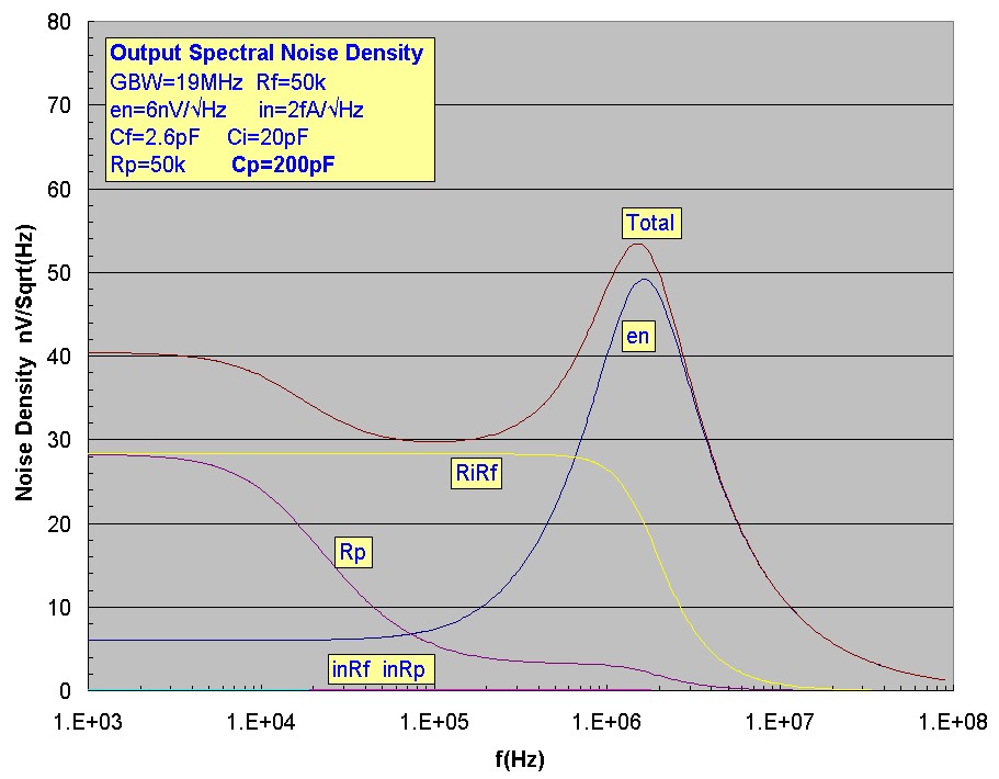
The output spectral noise voltages for each of the noise components are shown in the
next set of plots (note the different horizontal frequency range). The first plots show the spectral noise density for the well-filtered Cp=200 pF case, corresponding to the example and the total output voltage
noise plots. The roll-off of the Rp thermal noise density is evident.
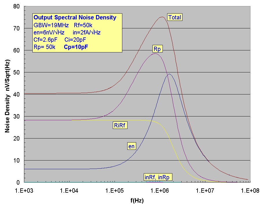
For comparsion, the final plots show the spectral noise for the unfiltered case with a residual Cp=10pF. The dramatic noise-gain peaking
effect on the gain experienced by the Rp thermal noise is evident:
The "compensated divider" condition is Cp = 22.6 pF. For Cp >200pF, the thermal noise contribution from Rp to the total output noise is negligible for these circuit values.
GBW = 19 MHz Cf = 2.6 pF Ci = 20 pF Rf = 50 kohm Rp = 50 kohm
en = 6 nV/√Hz in = 0.002 pA/√Hz
Fz = 141 kHz f3dB = 1.63 MHz
Cp (pF)     Vn(Thermal Rp)     Vn(en & Thermal Rf)    Vtotal (uV)

   10             75                77.2               108
   22.6           37                77.2                86
   50             19                77.2                79
  200              6                77.2                77.5
 1000              2                77.22               77.25


 Consider the following transimpedance circuit where Ip could represent the photocurrent of a photodiode.
Ci and Ri are the total input shunt capacitance and resistance at the inverting input.
In the following, it will be assumed that Ri >> Rf which is true in many cases.
It is common practice to use a bias-current compensation resistor Rp ~ Rf to cancel DC output offset errors originating form ib.
However, introducing Rp increases the output noise of the circuit since the thermal noise of Rp experiences the full noise-gain amplification,
including any noise-gain peaking effects originating from the noise-gain zero at Fz = 1/2πRf(Cf+Ci).
(Current noise in also contributes input voltage noise but will be ignored here assuming a FET-input device with extremely low in)
This contrasts with the thermal noise contribution from Rf which does NOT experience
the noise-gain peaking effect with the thermal noise of Rf merely being rolled-off by the feedback pole, augmented by the op-amp intrinsic bandwidth roll-off.