Fz: Noise gain zero frequency
Fp: Noise gain pole frequency
Fc: Intersection frequency of noise gain and open loop gain
Margin: Phase margin of loop gain at intersection frequency (stable for margin >45deg)
NG(Fc): Noise gain at intersection frequency Fc
f3dB: 3dB bandwidth relative to DC value
Q: Quality factor of resonant peaking
Fpeak: Frequency of resonant peaking
Peak: Resonant peaking value in dB
Cf(flat): Cf value for maximally flat (Q=1/Sqrt(2)) response for Tz and INV circuits, if possible
About The Noise Calculation for Tz Circuit
The input-referred noise-current densities and total integrated noise current In_tot, for a noise-bandwidth of Fp, and the output noise voltage Vn_tot are calculated for the transimpedance circuit configuration.
It is assumed that Ri >> Rf for the noise calculations. en is the op-amp input voltage noise spectral density and in is the op-amp input current noise spectral density. If the signal current source Ip
in the transimpedance circuit is a reverse biased device (such as a photodiode), the shot-noise due to that devices DC leakage current must also be included (see below).
If the pole frequency Fp is higher than the intersection frequency Fc, then Fc is used as the bandwidth for the total noise calculation since noise-gain rolls off starting at Fc. If the pole frequency Fp is considerably LOWER than the
intersection frequency Fc, Fp is still used as the bandwidth for total noise calculation which means that the circuit should be post-filtered to ensure the noise gain is rolled off at Fp for this noise estimate
to be valid and to eliminate extra noise. (Since the signal bandwidth rolls off starting at Fp, this output filtering will not impact signal output and will improve S/N ratio).
The expressions below are used to calculate each input-referred noise current density component and the total noise values:
The last term in the In_eq expression is a result of the noise-gain zero which gains-up the op-amp
noise voltage at frequencies higher than the noise-gain zero. Note that this current-density term is EXPLICITLY bandwidth dependent and can in many cases dominate the other noise
current components, particularly in high-bandwidth circuits with large input capacitance and high gain (Rf). The op-amp input noise current term and the thermal noise term of Rf don't experience
the same enhanced noise effect and their noise contributions start rolling off at about the pole frequency in a similar way to the transimpedance output signal voltage rolloff.
Generally speaking, to maximize transimpedance circuit sensitivity, it is desirable to use as high a gain (Rf) as possible provided there is enough signal bandwidth for the intended application and to choose an
op-amp with very low input voltage noise en and input capacitance to lower the gaining-up effect. For maximum sensitivity, the goal is to select an op-amp with low en, in and Cin to achieve a noise performance
in the Tz circuit which is limited only by the intrinsic thermal noise of Rf, for the particular photodiode and with the required bandwidth.
The diagram below which corresponds to the default parameters in the calculator above, shows how the noise-gain curve starts to increase (gaining up the op-amps voltage noise en at a rate of 20 dB/decade) above
the noise-gain's zero frequency ~ 1.7 kHz and continues to increase, raising the noise, and finally levelling off at the pole frequency 106 kHz and finally rolling off as limited by the op-amp GBW
limit:
For a more detailed discussion of noise considerations for transimpedance circuits, see:
Photodiode Amplifiers Op Amp Solutions, J. Graeme, McGraw Hill, 1996, p. 87.
The simplified noise calculation here, which assumes constant spectral densities for en and in over the bandwidth of interest, shows the size of each contributing noise current component and
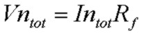
the total input-referred current density, total current density over the bandwidth Fp and the output total noise voltage which is In_tot*Rf.
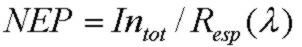
The total input-referred noise current provides a measure of the minimum detectable optical power for a photodiode receiver. A phodiode is characterized by a wavelength-dependent Responsivity (A/W)
which describes the conversion efficiency of received optical power to generated photocurrent. A typical value for responsivity in the red (wavelength ~ 650 nm) part of the optical spectrum would be ~ 0.5 A/W.
The optical power corresponding to the total input noise current of the transimpedance circuit is called the Noise Equivalent Power or NEP:
For example, for In_tot = 27 pA, and with Responsivity = 0.5A/W, the minimum detectable optical power in this Tz circuit with the specified bandwidth would be 54 pW.
Photodiodes are typically reverse biased to reduce junction capacitance. However a biased photodiode, like any reverse biased PN junction exhibits leakage ("dark") current. This dark current
introduces extra shot noise to the circuit characterized by a constant spectral density:
or, using convenient units:
Evaluation of this expression from the photodiode specifications will indicate if it contributes significantly to input-referred current noise. If so, it should be added to the RMS noise-current summation above.
Generally smaller photodiodes will have less dark current. For example the commercial Vishay Semiconductors BPW24R Si photodiode exhibits a dark current of ~ 3nA at reverse voltages of less than
10 V. This corresponds to a shot-noise current density of ~ 31 fA/Sqrt(Hz) (or 0.03 pA/Sqrt(Hz). In the default calculator example, this is comparable to the final noise-gain term.
The photodiode dark current will also contribute to an output DC offset voltage by an amount Id*Rf or for the 5 Mohm case above and a 3nA dark current, an offset of 15 mV.

 Fz: Noise gain zero frequency