Pulse Circuits for
Infrared LEDs and Visible Diode Lasers
M. Gallant Jan 02 2009
 This article demonstrates basic circuits for pulsing infrared LEDs and low power visible semiconductor lasers
using components which are inexpensive and fairly readily available. Many interesting and useful applications can be found
in the references cited here, as well as several online web pages. This article focuses on the basic circuits.
This article demonstrates basic circuits for pulsing infrared LEDs and low power visible semiconductor lasers
using components which are inexpensive and fairly readily available. Many interesting and useful applications can be found
in the references cited here, as well as several online web pages. This article focuses on the basic circuits.
The infrared LEDS fabricated from GaAs or GaAlAs discussed here are PN semiconductor junction diodes fabricated
from GaAlAs or GaAs and typically emit at wavelengths in the range 850 - 950 nm (with 880 and 915 nm being
two readily available choices). Uses include infrared remote controls for consumer appliances.
Typical specifications are DC optical power output ranging from 1 to 10 mW at DC forward
currents of 20 to 100 mA with forward voltages from about 1.3 to 1.7 V. Considerably higher peak power outputs
can be achieved if the LEDs are pulsed with short pulses in the range of 1 us to 100 us with low duty cycles of
1 to 10%. Optical pulse rise/fall times available from these LEDs range from ~ 500 ns to 20 ns (corresponding to
bandwidths on the order of 1 MHz to 20 MHz).
Visible semiconductor lasers found in common laser pointers emit at about 650 +- 20 nm and are commonly in
the Class IIIA Laser Product category, emitting less than 5 mW under DC bias conditions from 4.5 to 6.0 V powered
by three or four 1.5V button cells. (Visible LEDS at this wavelength are also commonly used in audio digital optical
output interfaces (S/PDIF) but power levels are only about 30 microWatts).Evidently the laser chips in most
low cost laser pointers use no protection or biasing circuitry at all and the chips are reported to have modulation
bandwidths of several hundred MHz extending the range of useful application considerably beyond that available with
pulsed LEDS.
Laser pointers can often be found at retail outlets at steep discount prices (often less than $5.00).

Many such pointers can easily be disassembled and pressed into pulsed service as demonstrated here.
However, due to the nature of the semiconductor laser device (high power density at the laser chip facet),
these emitters are susceptible to catastrophic damage due to transients current "glitches" in electronic pulser
circuits and care should be taken to study the electronic driver pulse signal, using suitable low value resistors,
before connecting the visible laser.
Photodectors suitable for studying pulsed infrared LEDS and visible diode lasers include high-speed Si PIN diodes with
fast rise and fall times of less than 10 ns. Si phototransistors offer high sensitivity (with current gain) but typically have
considerably lower speed, typically in excess of 200 ns.
The picture below shows 2 diode lasers (upper) extracted from laser pointers, two infrared LEDS (lower left) and a Si phototransistor (TIL 99) :

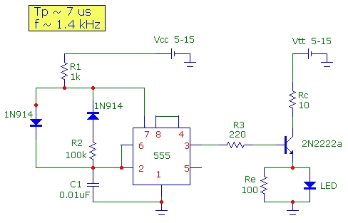
High Current Infrared LED Driver
Many infrared GaAlAs LEDS can be driven at currents approaching 1000 mA provided that the duty cycle and pulse width is
short enough to keep the average power dissipation low enough. Using a standard 555 timer IC and a 2N2222a NPN transistor,
it is possible to create a drive pulse with width down to a few microseconds and amplitude to about 800 mA.
The 555 timer chip has a rise/fall time of about 100 ns and current drive capability of 200 mA. The transistor output driver raises
the output drive capability by about a factor of 4.
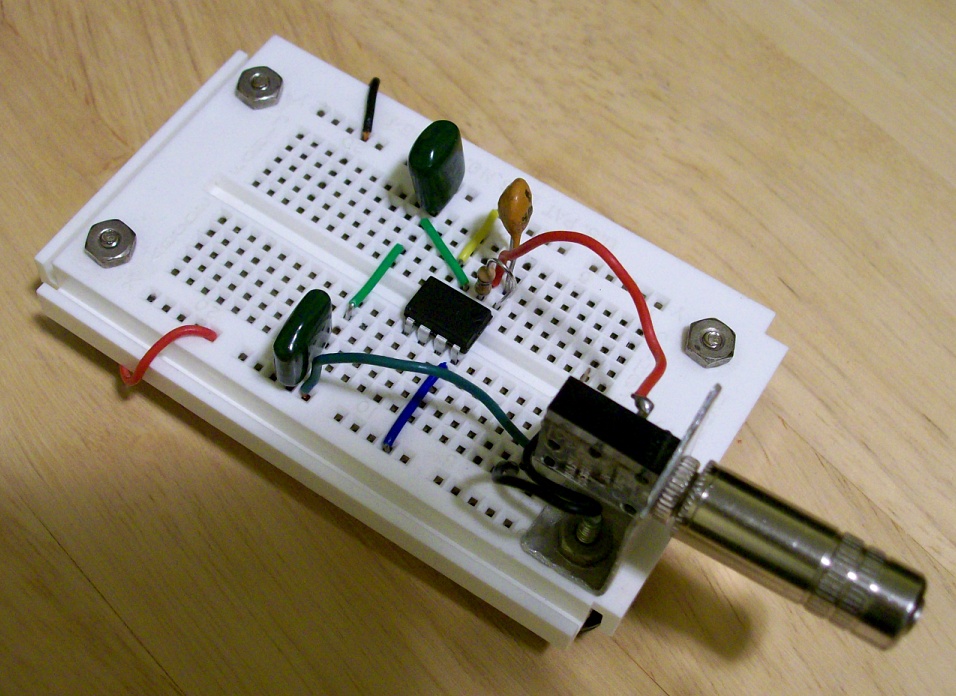
The diagram below shows an implementation of this approach. The 555 timer circuit uses 1N914 switching diodes to enable complete
control of the on/off time for the pulse. Despiking and power supply decoupling capacitors of 0.1 and 5 uF were used.
A 220 ohm series resistor in the 2N2222a base circuit is used to set the base drive level.
A 10 ohm collector resistor provides suitable current limiting.
The LED in the emitter circuit is shunted with a parallel 100 ohm shunt resistor to speed up the fall time of charge
drain.
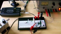
The 555 and transistor were biased at the same adjustable level with a common power supply (22-121 Micronta Adjustable Dual Tracking
DC power supply rated at 1 Amp and 15 V).
The LED drive pulse and the PIN photocurrent were monitored using a
Syscomp Electronic Design DSO-101
dual channel 2 MHz (~ 100 ns risetime) compact USB oscilloscope:

The optical pulse was detected using a reasonably low capacitance (50 pF @ -3 V bias) Si PIN detector amplified with a
National LM4562 opamp
current-to-voltage converter circuit.
With a 55 MHz GBW and a slew rate of 2V/100ns, a feedback resistor Rf of 10 kohm provides good signal amplitude with
a just sufficient 3dB closed-loop bandwidth of 4 MHz (88 ns tr/tf) for optical detection.
A feedback shunt capacitor of 5 pF across Rf suppresses gain peaking.
(Rf of 1 kohm enables 16 MHz BW with a 10 pF peaking capacitor;
Rf of 220 ohm enables 28 MHz BW with a 20 pF peaking capacitor). Care should be taken in the component layout to minimize
wire lengths to reduce stray capacitances, particularly around the feedback resistor.
In addition, this opamp can be used with power supplies as low as +_2.5 V. In this work for convenience 4-AA batteries were used to provide +_ 3.0 V with clipping at 2.5 V.
The detector was used in photoconductive mode with -3V applied to lower capacitance and improve linearity.
Using a SEP8703-001 880 nm LED (Radio Shack/The Source # 276-143a), the following LED drive current results are achieved:
Vcc= 5.0 Ic = 250 mA
Vcc=10 V Ic = 600 mA
Vcc= 14.5 V Ic = 820 mA
For drive currents less than about 200 mA, the 555 alone can be used, with a suitable current limiting resistor.
Scope display showing collector voltage (blue) and PIN photocurrent at Vcc=10 V Ic = 600 mA. LED pulse rise/fall times are on the order of 500 ns:

Scope display showing Vbase of 3.2 V at Vcc= 10 V Ic=600 mA. The corresponding Ve (LED) voltage level is about 2.0 V :

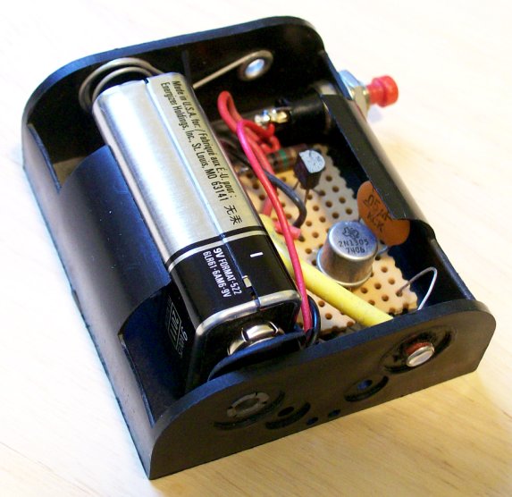
If higher current pulses are required (1000 - 2000 mA) but less control over the pulse shape can be tolerated, then a very simple
discrete solution is a 2 transistor flip-flop circuit using a Si and Ge transistor (e.g. 2N2222a and 2N1305). Some infrared LEDs can be driven to
2 Amps with 1% duty cycle in this way. See Forrest Mims Circuit Scrapbook for a good discussion of this approach. The image below
shows an example mounted in a dual C cell holder:
Visible Diode Laser Low-Speed Driver
For longer pulse widths and with rise/fall times no shorter than 200 ns, the 555 timer chip can be used to directly drive a visible diode laser at the
nominal current level (usually 20 - 30 mA) with a current limiting series resistor. The drive pulse shape should be examined carefully using a load
resistor simulating the laser to ensure that drive spikes from the 555 timer are not excessive. Wiring from the 555 to the laser should be short
to minimize inductive effects which can cause ringing. The result below shows an example using only the
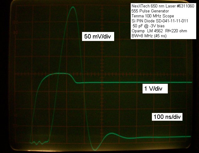
555 part of the circuit above with the same 220 ohm series resistor to directly drive the laser removed from a Nexxtech 6311060 Mini Laser Tool Set.
The lower blue trace is the laser voltage (6V peak drive value). The upper red trace is the Si PIN/opamp voltage signal.
The much faster optical rise/fall time compared to the infrared LED is obvious. A slight overshoot on the drive pulse is evident in the fast optical response:

The voltage overshoot of the 555 can be used as a crude way of obtaining an optical pulse of about 200 ns in width based on the steep I-V curve. If the laser is pulsed
to just slightly above threshold, the overshoot will generate a narrow pulse as shown below:
The setup below shows the visible laser mounted in a box (background). The beam is directed to a tilt-mount mirror about 1 meter in the forground (not visible)
and reflected back onto the pin photodiode (in forground):

To obtain an optical pulse from a visible diode laser significantly shorter than a few microseconds and with rise/fall times faster than 100 ns, faster drive electronics must be used.
A simple example of one approach is shown below.
Visible Diode Laser Medium-Speed Driver
Assuming a typical visible diode laser can be digitally modulated at rates of several hunded MHz, then optical pulse risetimes of nanoseconds
should be possible.
Designing fast driver electronic circuits in this range requires a good understanding of the laser response characteristics and high-speed electronics.
It is possible however to produce drive pulses in the 20 to 100 ns range fairly easily using standard TTL or CMOS circuits.
The following circuit shows one simple approach using a 555 timer chip (~100 ns switch time) and a TTL inverter (~ 10 ns switch time):
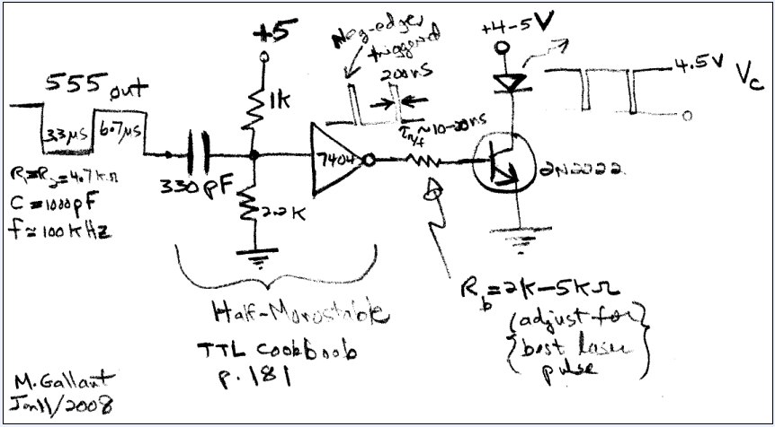
The 555 timer generates pulses of several microseconds in duration with ~ 100 ns rise/fall time. The standard TTL 7404 hex inverter has a switch time on
the order of 10 ns. In the circuit above, 1/4 7404 is used as a "half monostable multivibrator" in which the inverter is triggered only on the falling
edge of an input TTL level pulse (see TTL Cookbook).The width of the inverter output pulse is determined by the two resistors and input capacitor of the inverter. In the
example above, a pulse of about 200 ns is created and the rise/fall time should be on the order of 10-20 ns. Since the output voltage of the 7404 is
limited (slightly less than 5 V in TTL) and visible diode lasers can typically require 5 - 6 V drive, a 2N2222a drive transistor is used again. However,
the laser must be placed in the collector circuit due to the higher voltage requirement of a visible laser (compared to an infrared LED). Also, it
is important to determine the correct base drive level in order to just achieve the required transistor switch saturation level; otherwise the 2N2222a
drive pulse with be widened due to charge storage effects. The 2N2222a has tr/tf of 20-50 ns but potential charge storage effects can easily
cause pulse broadening to hundreds of ns. A transistor biasing pulsed simulation programme such as MicroCap helps in determining a good
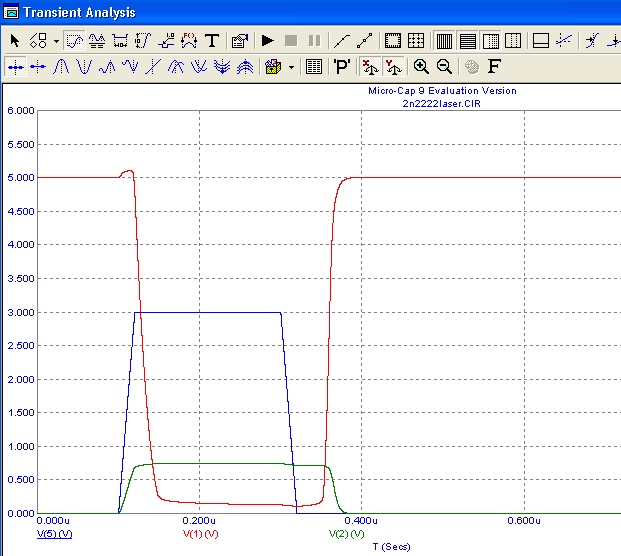
operation point for fast pulse generation. The diagram below shows a simplified model of a CE 2N2222a circuit with a pulsed input voltage source (representing
the 7404 output). The laser is crudely modeled as a fixed resistor of 220 ohm in the collector circuit corresponding to a laser with Vf=4.5 V at If=20 mA:

The transistor biasing conditions (voltage level and resistor values) can be adjusted in the simulation to determine the sufficient drive to produce the best
shaped collector voltage pulse:
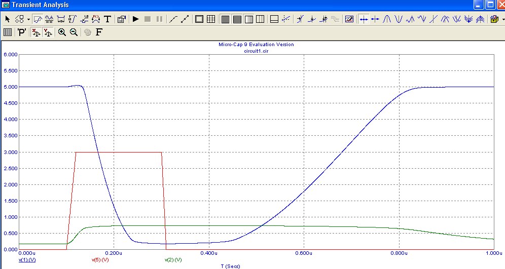
Overdriving the transistor in this configuration leads to pulse lengthening and a degraded fall time as shown in this simulation:
With proper biasing a reasonably fast 100 ns pulse with tr/tf ~ 20 ns is achieveable. The scope trace below shows measured results for the
555-->7404--->2N2222a circuit with transistor voltage-divider biasing resistor values of 220/100 ohms. In this case, a 650 nm visible diode laser
from a laser pointer with a nominal DC bias of 4.5 V at 20 mA was used.
The upper trace (blue) is the collector voltage showing a just resolved sharp 200 ns drive pulse with 4.5 V swing. (The time response in these results
is limited by the scope bandwidth).
The lower trace shows the Si PIN photodiode signal showing a similarly fast optical pulse.

Using a modest commercial function generator and a 100 MHz scope, the trace below shows a pulse width at least as short as 80 ns (limited in this case by the 40 ns tr/tf
of the detector/opamp combination) can be achieved using an ordinary visible diode laser:

High Radiance Infrared LED Driver
A reasonably well-shaped 20 nS pulse for driving an infrared high-radiance LED can be built using a 2N2369a avalanche
transistor circuit. This transistor when operated in the avalanche breakdown region, can be used to generate
sub-nanosecond pulses for various applications including testing high-speed oscilloscopes. An assembled circuit and the
output 10 V pulse with 600 ps tr/tf is shown below for a 2N2369a transistor with an avalanche breakdown voltage of 60V.
The output pulse height will depend somewhat on the exact breakdown voltage of the 2N2369a with a range
of 60 to 85V typical, depending on the manufacturer and lot number. A suitable low current 100 VDC power supply
can be assembled easily using a 115VAC/25VAC transformer or adapter and a voltage tripler circuit.


The collector capacitor C1, which is typically 2 - 5 pF for subnanosecond pulse generation, charges through the collector
resistor R5 until the transistor breaks down, discharging C1 through the transistor and paralleled emitter resistors thereby
generating a short voltage pulse. The collector voltage trace below shows the charging and avalanche-breakdown and discharge
cycle. A x10 attenuation probe was used and the voltage source was 100 VDC. The breakdown voltage for this
device was 82V.
However, high radiance fast LEDs typically have response times on the order of tens of nanoseconds. The avalanche transistor
circuit can be combined with a simple pulse-shaping approach using an inductor
to provide 100 mA /10 ns drive current pulses at a low duty cycle (<1%).
The circuit schematic and breadboarded layout are shown below:


A 1N914 Si signal diode in shunt across the LED helps clean up the fall time of the pulse.
Without the LED connected, the electrical pulse across the output 50 ohm resistor is shown below:

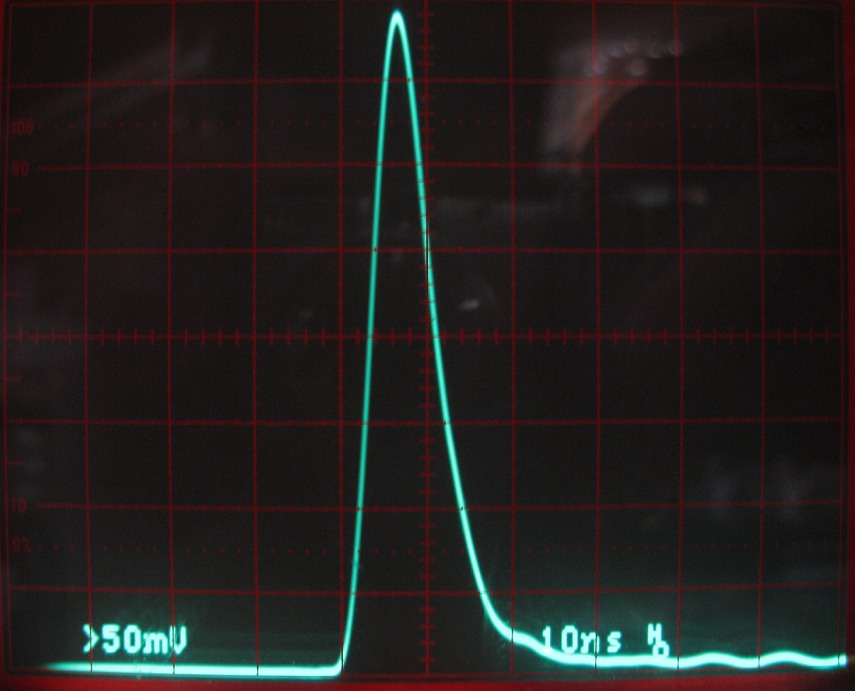
With the LED connected, and the optical output pulse from an 870 nm high-radiance
Vishay TSFF5210 LED
is shown below, as detected with a
Thor Labs PDA10A
150 MHz bandwidth high-speed Si photodetector:

For an example of a 50 MHz bandwidth analog LED modulator, see LED Modulator Circuits.
High-radiance infrared LEDs such as the Vishay TSFF5210 AlGaAs LED shown to the right
can be driven to peak current levels up to 1 Ampere provided the pulse width is less than
a few microseconds and the duty cycle is one percent or less.
For example, the TSFF5210 high-radiance 870 nm LED is specified with a radiant optical power of 50 mW
at 100 mA and over 250 mW at 1Amp drive current. Of course the ability to make use of these high optical power
levels in practice depends on designing good coupling optics (i.e. lenses with suitable numerical aperture).
Using a current booster high-speed switching output transistor, very high output optical levels
are possible. In the circuit shown below, another 2N2369a was used as the current booster. 2N2222a transistors
can also be used with smaller and somewhat wider output pulses:

The LED peak drive current level for the components shown is about 800 mA with a duty cycle of ~ 0.5%. Due to the very high
level of saturated switching, the pulse width broadens from about 20 ns to 40 ns. The output pulse is also more symmetrical
than the input pulse:

To verify the high emitted optical power from the LED under a drive current of 800 mA, the detector with an active area diameter
of 1mm was moved 35 mm from the LED emitting source. At this distance, the peak photodiode signal
voltage was measured to be 1.1 V.
The half-angle subtended by the detector is ATAN(0.5/35) or
0.82 deg corresponding to a solid angle or 6.4x10⁻⁴ steradians (sr). The LED specification sheet claims a radiant intensity
of about 1400 mW/sr at 800 mA. Therefore the power received by the photodiode should be 6.4x10-4 X 1400 or about 0.9 mW.
The PDA10A photodetector has a responsivity of 0.25 mA/mW at 870 nm and a transimpedance gain (into 50 ohm)
of 5V/mA providing a photodetection sensitivity of 1.3 V/mW. Therefore a received peak power of 0.9 mW would be detected
as a 1.2V peak pulse which is close to the 1.1 V measured result. This confirms the high radiant intensity achieved under these conditions.
A simplified circuit simulation using the component values in the circuit above is shown below.
The avalanche transistor breakdown pulse source is simulated simply as the
capacitor C1 charged initially to 70V (the breakdown voltage). The bias voltage V1 for the output current boost switching
transistor is 10V. The infrared LED is modelled as two Si switching diodes in series:


It is possible to simplify the avalanche breakdown driver circuit by removing the pulse-shaping inductor, and placing the IR LED directly
in the 2N2369a emitter circuit, provided that care is taken not to exceed the LED peak low duty cycle current of 1 Amp. In this approach greater
collector capacitance is required to achieve high pulse currents and the results will depend more on the specific
2N2369a transistor used. Also an LED shunt resistor should be used so that the
emitter circuit contains a low resistance path during the avalanche breakdown decay. A 51 ohm shunt resistor works well as shown in
the circuit below:
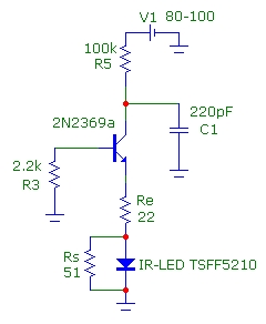
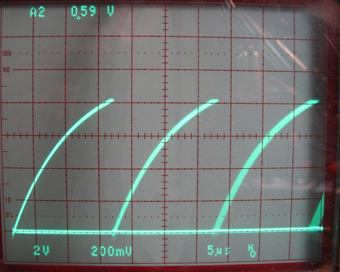
With C1 = 220 pF and Re = 22 ohm, good results were obtained with Motorola 2N2369a transistors. A peak pulse current
of about 900 mA was measured. An optical pulse width of 40 nS was observed using a 23 MHz bandwidth Vishay TSFF5210 LED.
A Vishay BPV10 250 MHz high-speed Si photodiode with tr/tf = 2.5 ns and biased at -30V with a 50 ohm load was used for optical detection.
The peak emitter and LED voltages during the pulse were 26 and 4.2 V respectively.
The resistor Rs therefore shunts about 80 mA of the total 990 mA of breakdown emitter current. By changing C1 to 100 pF, a somewhat narrower
pulse of 25 nS is achieved with a lower peak current of about 600 mA.

Visible Diode Laser High-Speed Driver
To obtain laser drive pulses on the order of a nanosecond or less, ECL fast logic or other series high-speed digital logic are possibilies. At these speeds, very
careful layout design is critical and switching transients must be carefully suppressed to prevent laser damage.
References
- "Optoelectronic Devices Data Book", Hitachi Publication, 1988
- "The Electro-Optical Components Data Book", 1977, TI Staff Publication
- "Understanding Optronics", Staff of TI Learning Center, 1981, Radio Shack
- "Silicon Photovoltaic Detectors and Detector/Amplifier Combinations", EG&G Application Note D3011C-6, 1982
- LM4562 - Dual High Performance, High Fidelity Audio Operational Amplifier
- "TTL Cookbook", Don Lancaster, SAMS, 1991, pp.171-181
- "Small-Signal Semiconductors" Q4/87, Motorola data book, 1987
- "The Forrest Mims Circuit Scrapbook", Forrest Mims, McGraw Hill, 1983, p 57
- "IC Timer Cookbook", Walter Jung, 2nd Edn. SAMS 1983
- "RCA Electro-Optics Handbook", RCA Publication, 1978
- "Optical Communication Systems", J Gowar, Prentice/Hall International, 1984
- "Electronic Principles" 3rd Edn, A. Malvino, McGraw Hill, 1984, p 488
- "Understanding Lasers", Jeff Hecht, 1988, Radio Shack
- "Engineer's Notebook II: Integrated Circuit Applications", Forrest M. Mims III, 1982, Radio Shack
- "Engineer's Mini-Notebook: Digital Logic Circuits", Forrest M. Mims III, 1986, Radio Shack
- "Engineer's Mini-Notebook: 555 Timer IC Circuits", Forrest M. Mims III, 1984, Radio Shack
- "Engineer's Mini-Notebook: Op Amp IC Circuits", Forrest M. Mims III, 1985, Radio Shack
- "Engineer's Mini-Notebook: Optoelectronic Circuits", Forrest M. Mims III, 1986, Radio Shack